Methodology and modelling
The boost converter (figure 1), is a type of DC-DC converter that can provide an output voltage greater than the input voltage [7]. Due to the conservation of energy, the input power of the boost converter must be equal to the output, which means that the current at the boost's output is less than the input current. This sort of converter is frequentlyutilized in PV applications due to its high efficiency and ease of implementation [8].
 Fig. 1
Conventional Boost Converter(8(
Fig. 1
Conventional Boost Converter(8(
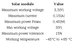
Since the aim of this study is to reduce the size and maintain the performance, a small solar panel containing polycrystalline coated solar cells protected by a solid outer frame was used, which has the characteristics mentioned in table 1.
Table 1
Characteristics of the used solar panel [9]
a) Design of DC DC converter
As shown in the figure 2, a Boost converter including a PV voltage source, an inductor L, a switch, a capacitor C and a load resistor R. In practice a MOSFET and Diode are used instead of switches. The switch of the boost converter is controlled with a PWM signal. Two operational modes arise from turning the switch “ON” and “OFF” with the PWM signal. The explanation of the boost converter and PWM is offered in detail in [10].
The input and output voltage relationship is controlled by the switch duty cycle, D, according to the following equation (1), [11]:
Where
Vinis the input voltageVoutis the output voltageDis the Duty cycle
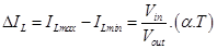
To operate the boost converter in this study we chose the continuous connection mode (CCM), hence the current in
the inductor (IL) never drops to zero, as shown in equation (2).
An expression for ripples IL (t) is extracted from the equation (3).
 Fig. 2
Solar PV integrated with DC-DC boost converter
Fig. 2
Solar PV integrated with DC-DC boost converter
b) Dimensioning of the spiral inductor
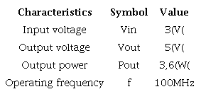
The dimensions of the inductor to be integrated in the boost converter will be determined by the characteristics indicated in table 2.
Table 2
Converter specifications
The calculated value of inductance is given by the equation (4):
Where
LInductance (H(
VinMinimum input voltage (V(
DDuty cycle
fSwitch frequency (Hz((I
LINDUCTOR CURRENT RIPPLE (A(
The maximum duty cycle for the boost converter is given by the equation (5):
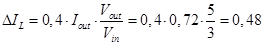
Since the inductor current ripple is unknown, it must be calculated using the equation (6):
To calculate the value of inductance we use equations (5) and (6), in equation (4):
A bigger diameter wire should be used for the coil, in order to reduce inductance DC conduction losses. Also, a lesser switching frequency should be selected, to decrease substrate losses. Both of these outcomes will create a physically bigger inductor that may be more expensive but will attain superior efficiency [12, 13]. One more consideration is the form of the inductor. Figure 3, shows the geometric parameters of a planar spiral inductor. These parameters are: width of the conductor (w), spacing between conductor (s), number of turns (n), thickness of the conductor (t), Innerdiameter (din) and outer diameter (dout).
 Fig. 3
Schematic of square spiral inductor [14]
Fig. 3
Schematic of square spiral inductor [14]
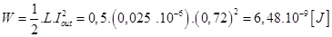
The magnetic energy stored is given by equation (7):
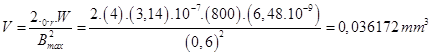
The volume of the magnetic material (NiFe) is calculated by equation (8):
Where, relative permittivity of (NiFe): (r = 800, saturation induction Bmax = 0.6
In order to calculate the area (A), we set the outer diameter (dout) of the inductor with a length of 2400[(m] and inner diameter (din) equal 1200 [(m].
Since the inductor is square in shape, we extract from equation (9), the following:
To calculate the number of turns for inductor we use Wheeler equation (10):
For a square inductor winding, the coefficients K1 and K2 are as follows 2.34 and 2.75.
The next ties define the form factor and the mean diameter by the following two equations (11) and (12), [15]:
Equation (13), is extracted from equation (10), (11) and (12):
It depends to extract the width and thickness of the conductor on the following condition: (w(2() o (t(2()
Where, δ is the skin thickness and obtained by equation (14), [16].
Where ( represent the resistivity of the conductor, ( Copper = 1.710 - 8 [(m] and μ its magnetic permeability. By fulfilling the condition (t(2(), t is obtained as follows t=13[µm
The width of conductor w is derived from the equations (15):
Where, S represent the conductor section and is equal to 1755 [mm2]. By applying the calculation to equation (15), we get the value of the width of conductor, which is equal to w=135[μm(
The spacing between conductors is expressed by the equation (16):
The length of the trace is expressed by the equation (17):
After calculations, we obtain the values of the dimensions of the spiral inductor, summarized in the following table 3:
Table 3
The geometric parameters of the inductor

We have considered the equivalent circuit shown in figure 4.
 Fig.4
(a) Transverse section of a spiral inductor, (b)Electrical circuit equivalent in ( of a spiral inductor [17]
Fig.4
(a) Transverse section of a spiral inductor, (b)Electrical circuit equivalent in ( of a spiral inductor [17]
This electrical parameters of spiral inductor are calculated using the formulas [18, 19], found in table 4, which will serve as the mainstay for the optimization and simulation.
Table 4
Formulas for electrical parameters

where
toxis the oxide thickness between the spiral and the substrate (
tox=30 μm)(
cuis the resistivity of the metal ((
cu=1,7 . 10
-8 (m
εoxis the oxide permittivity (
εox=3,9) (
ε0=8,85 pF.m
-1)
hsubis the substrate height (
hsub=50 μm)(
subis the substrate resistivity ((
sub= 18,5 (m)
εsubis the substrate permittivity (
εsub=11,8)(
δ)is the skin depth(
μ)is the magnetic permeability of free space
Simulation of magnetic behavior
To get closer to reality and based on the results of the dimensioning as shown in table 2, we will show the geometry of our spiral inductor model designed in 3D as shown in figure 5.
 Fig. 5
Structure of the spiral inductor simulated with the mesh of the field of study
Fig. 5
Structure of the spiral inductor simulated with the mesh of the field of study
a) Distribution of electric potential and magnetic flux density
Figure 6, shows the distribution of the current density and magnetic flux density in the square planar coil in 3D.
 Fig. 6
(a) 3D view for the magnetic flux density, (b) 3D view shows the current density
Fig. 6
(a) 3D view for the magnetic flux density, (b) 3D view shows the current density
b) Selection of the optimal frequency
To keep the conductor size within the appropriate range, the optimum frequency f should be chosen to limit overheating due to skin effect or lack of energy due to large losses. As such, the simulations was carried to observe the magnetic flux and the current density of three different frequencies: [1 kHz, 2223 kHz and 5001 kHz]. The simulation results are shown in figure 7. It’s noticeable a considerable augment in magnetic flux density for more frequency; this is correlated to the density of electric current in the conductor, which is more important in added frequency (figure 8).
 Fig. 7
Simulations of the current density norm according to the arc length mentioned in spiral inductor
Fig. 7
Simulations of the current density norm according to the arc length mentioned in spiral inductor
 Fig. 8
Cross-sectional plot magnetic flux density along the arc length mentioned in spiral inductor
Fig. 8
Cross-sectional plot magnetic flux density along the arc length mentioned in spiral inductor
c) Simulation of the electric model of the photovoltaic system
Figure 9, shows the simulation circuit of a photovoltaic system with a boost converter containing the electrical circuit of integrated spiral inductor model (figure 4):
Figure 10, shows the current flowing in the inductor and the voltage and current produced by the boost converter. The obtained simulation results show us that the output voltage Vout and the output current Iout are continuous, The obtained values are fairly close to the specification of the boost converter DC-DC. These results show that the spiral inductor integrated into the boost converter works well. Thus, we can ensure that the geometric dimensions of the integrated spiral inductor and its electrical parameters are well defined.
Figure 10(a), shows the simulated output current (Iout) at a switching frequency of 100 MHz. It is noted that the output current is constant starting from the first 40 [ms]. The boost converter delivers an output current of about 0,72 [A]. In addition, a similar observation is observed for the output voltage (Vout) as shown in figure 10(b), where the mode is transient in the first 20ms. Also, we notice that the output voltage increased from 3[V] to 5[V]. The waveform current across the inductor terminals shown in figure 10(c), never crosses the zero value, where this change ranges between 0,4829 [A] and 0,4871[A]. Therefore, the continuous conduction mode is respected.
 Fig.9
Photovoltaic system and boost converter with an integrated spiral inductor
Fig.9
Photovoltaic system and boost converter with an integrated spiral inductor
 Fig. 10
Waveforms in boost converter, (a) Output current, (b) Output voltage, (c) Current flowing in the spiral inductor
Fig. 10
Waveforms in boost converter, (a) Output current, (b) Output voltage, (c) Current flowing in the spiral inductor
 Abdelhadi Namoune abdelhadi.namoune@curelizane.dz
 (1)
(1) (2)
(2) (3)
(3) (4)
(4) (5)
(5) (6)
(6)
 (7)
(7) (8)
(8) (9)
(9) (10)
(10) (11)
(11) (12)
(12) (13)
(13) (14)
(14) (15)
(15) (16)
(16) (17)
(17)