Articles
Parallel-charge series-discharge inductor-based voltage boosting technique applied to a rectifier-fed positive output DC-DC converter
Parallel-charge series-discharge inductor-based voltage boosting technique applied to a rectifier-fed positive output DC-DC converter
Journal of applied research and technology, vol. 18, no. 5, pp. 229-244, 2020
Universidad Nacional Autónoma de México, Instituto de Ciencias Aplicadas y Tecnología
Received: 20 March 2020
Accepted: 22 May 2020
Published: 31 October 2020
Abstract: The conventional power electronic boost converters have inherent limitations that they are not able to increase the low DC input voltage level into sufficiently high DC output voltage level. This is because of the fact that (1). the inductor used in the converter has certain amount of internal resistance, and (2). the power devices used in the converter are subjected to high potential stress which led to damage of the devices. A configuration of a non-isolated step-up rectifier-fed positive output power converter capable of converting low DC voltage into high DC output voltage-based on the concept of parallel-charge series-discharge inductors is proposed in this paper. The proposed converter is fed by an uncontrolled diode bridge rectifier to which an input sinusoidal AC voltage of magnitude 30 V (rms) is given. The converter is configured such that the input AC voltage of 30 V (rms) is stepped-up to around 900 V (DC) at the output of the converter, with extremely low duty ratio. The proposed converter configuration employs only two high power semiconductor switches with reduced complexity of control. In this work, the converter topology is presented, and its steady state behavior and dynamic modeling are discussed for continuous inductor current mode operation. Further, it is revealed that the voltage gain of the converter is influenced by the variation of the duty cycle of the power switches. The effectiveness of the converter is better understood through simulation in MATLAB/SIMULINK platform. The results demonstrate that the converter is able to maintain higher constant output voltage profile with significantly reduced overshoot and settling time.
Keywords: Continuous inductor current mode, Discontinuous inductor current mode, Duty cycle, Dynamic modeling, MATLAB/SIMULINK, Parallel-charge series-discharge inductors, Positive output power converter, Steady state modeling, Voltage gain.
1. Introduction
In recent advancements, DC-DC power electronic boost converters have had a significant role in various applications such as hybrid electric vehicles, fuel cell energy conversion systems, medical equipment, military applications, battery charging and many more, where the high DC output voltage is obtained with the high ON time of the power switches. However, the high ON time (high duty cycle) led to certain issues such as reduced efficiency of power conversion, high potential stress across the switches, severe reverse-recovery issue of diodes, and electromagnetic interference problems (Hsieh, Chen, Liang, & Yang, 2012; Yang, Liang, & Chen, 2009). The conventional boost converters may be cascaded to increase the DC output voltage level with low value duty cycle operation (Prabhala, Fajri, Gouribhatla, Baddipadiga, & Ferdowsi, 2016; Wai, Lin, Duan, & Chang, 2007). While cascading, the efficiency of power conversion gets decreased. Another disadvantage is that the increased potential stress appearing across the power switch and the diode at the output stage. A single switch-based concept of cascading two boost converters was used in the quadratic converter. But this type of converter employed inductor and capacitor of higher ratings and suffers from the high potential switch stress. Several stacked converters are introduced by some authors to increase the voltage gain (Dwari & Parsa, 2011; Wu, Chen, Yang, & Kuo, 2010). However, these types of converters also suffer from the disadvantage that the capacitors at the output need to maintain voltage balance across them particularly when their number is increased. The voltage stress appearing across the output diode of the conventional boost converter can be mitigated using three levels in the conventional converter and the increase in effective frequency can reduce the size of inductors (Yaramasu & Wu, 2011). This converter is impracticable for certain applications due to the insufficient voltage level at the output.
There are certain types of isolated power electronic converters which utilize the concept of adjusting the number of turns on the primary and secondary side of the transformer to obtain the increased output voltage levels. However, the high leakage inductance of the transformer and increased potential switch stress limit the applications of these converters. Some authors developed certain converter configurations that are able to produce high DC output voltage, high power conversion efficiency and reduced switch stress by utilizing magnetically coupled inductor along with transformer (Duarte et al., 2013; Evran & Aydemir, 2014; Forouzesh, Siwakoti, Gorji, Blaabjerg, & Lehman, 2017; Tofoli, de Castro Pereira, de Paula, & Júnior, 2015). But many converter topologies that can improve both the voltage gain and efficiency are presented in the literature (Chub, Vinnikov, Blaabjerg, & Peng, 2016; He & Khaligh, 2017; Hu & Gong, 2014; Tseng & Huang, 2014).
It is also possible to reduce the switch stress along with improved output voltage level if voltage multiplier cells are hybridized with the conventional single switch power converters. The conventional, Cuk and SEPIC DC-DC converters employ voltage multiplier circuitry (Chub et al., 2016). The conventional step-up converter’s gain may be increased N times by a power electronic converter which is capable to produce inverting DC output voltage (Mahajan, Sanjeevikumar, Ojo, Rivera, & Kulkarni, 2016). Further, there are power converters that employ interleaved boost concept to increase the DC output voltage level with reduced ripples in the output voltage and output current (Bhaskar, Kulkarni, Padmanaban, Siano, & Blaabjerg, 2016). Some authors proposed the concept of interleaved multilevel voltage multiplier-based power converter topologies that are capable to produce 2N and 4N times the output voltage level of conventional boost topology (Bhaskar, Sanjeevikumar, et al., 2016). But, this high output voltage level is influenced by (i). balancing of voltages across the various capacitors with suitable time constants, and (ii). more number of diodes. The charge and discharge characteristics of the capacitors influence the power conversion efficiency (Bhaskar, et al., 2016). Two or more conventional boost converters can be connected in parallel using interleaving technique. This interleaving technology can easily cause the filtering of ripples in the input current (Li & He, 2011; O’Loughlin, 2006; Roy & Ayyanar, 2017). The range of DC output voltage can be increased using coupled inductors along with voltage multiplier units (Rosas-Caro et al., 2011). However, while using coupled inductors concept, energy circulation and snubber circuits are required to reduce the potential stress across the switches.
Switched capacitor (SC)-based converters, having high efficiency with good output voltage regulation and low weight, mainly consist of large number of switching devices and capacitors with various ratings, and the output voltage level can be boosted by the charge and discharge characteristics of capacitors (Mahajan, Sanjeevikumar, & Blaabjerg, 2017; Qian et al., 2012). The use of large number of switching devices leads to high switching losses. Hence, the efficiency of the SC-based DC-DC converter cannot be improved due to large power rating of the switching devices. Moreover, the increase of voltage gain of the converter is also limited. The SC-based converter circuits can have higher energy and power densities since they do not use reactive elements for energy transfer. Moreover, the SC circuit can be fabricated into an integrated chip (IC) and mostly used in low-power electronics applications.
There is another possible solution for improving the DC voltage gain of the converter using switched inductor (SI)-based DC-DC conversion technology, which employs parallel-charge and series-discharge inductors (Yang et al., 2009; Gautam, Sharma, & Shukla, 2019). This switched inductor-based converter configuration can operate in boost mode as well as in buck-boost mode. When it is operated in boost mode, then the configuration is called switched inductor boost converter (SI-BC), and in buck-boost mode, it is called switched inductor buck boost converter (SI-BBC). These configurations employ only a single active switch. But the switch is subjected to high voltage stress. Both the SI-BC and SI-BBC configurations are capable to improve the voltage gain by (1+Duty ratio) times and two times compared to the respective conventional DC-DC converters.
Some authors proposed a high step-up DC-DC converter structure consisting of a full-bridge module and the Cockcroft-Walton principle-based voltage multiplier to achieve high voltage gain in photovoltaic applications (Hossain, Selvaraj, & Rahim, 2018). A quasi-switched boost inverter configuration with voltage multiplier cell can be used for achieving high voltage gain with decreased voltage stress on the switches (Nguyen & Chai, 2019). A non-isolated approach of LLC resonant DC-DC converter with balanced rectifying current and stress has been proposed by some authors (Dobi & Sahid, 2020). This configuration has significantly reduced transformer loss because of non-isolation. The PI controller-based super lift technique applied to DC-DC Luo converters has been proposed by some authors to improve the voltage conversion ratio (Adlakha, Khosla, & Joshi, 2020) in which the comparative analysis of various positive output super lift DC-DC Luo converters is discussed. A non-isolated high voltage gain DC-DC converter proposed in (Saravanan & Ramesh Babu, 2019) is compared with boost, SEPIC and modified SEPIC converters. The converter proposed in (Saravanan et al., 2019) shows high efficiency compared to the other converters.
In this work, a diode rectifier-fed positive output power electronic converter, capable to increase the DC output voltage to the higher level without using high duty ratio of the switches, is analyzed theoretically and using simulation software. Here, three identical inductors each of value 0.1 mH are used. The concept of parallel-charge and series-discharge characteristics of the switched inductors is used to increase the DC output voltage level to the higher value. It employs only two power semiconductor switches which are subjected to low voltage and current stresses during the switch-off and switch-on periods. There are certain assumptions to be made for the analysis of the proposed converter:
- 1. The diodes and MOSFETs used in the converter have negligible forward voltage drops and are having negligible resistance during forward conduction mode. The inductors and capacitors used are lossless.
- 2. Large capacitances are assumed for the capacitors to maintain constant voltages across them.
- 3. The current flow through the three inductors in the proposed configuration increases or decreases linearly.
The remaining sections are arranged in such a way that the proposed work is illustrated effectively. The section 2 describes the configuration and various modes of operation of the converter under study. The MATLAB / SIMULINK model of the converter and its time domain simulation results are discussed in section 3. The conclusion for the proposed work is given in section 4.
2. Configuration and modes of operation of the converter under study
The topology of a rectifier-fed non-isolated high step-up positive output converter capable of producing high DC output voltage is shown in Figure 1. The single-phase AC supply of 50 Hz frequency is fed to a diode bridge rectifier which gives an uncontrolled DC voltage. The ripples in the DC voltage are filtered by a capacitor. The filtered DC output voltage is acting as source to the DC-DC converter stage whose output is filtered by a capacitor C0. The converter output voltage appears across a load RL . The proposed converter employs three identical inductors of inductances L1, L2 and L3 respectively. The two high power semiconductor switches S1 and S2 are triggered simultaneously into conduction by proper gate signals. The theoretical waveforms of the rectifier-fed converter operating under continuous and discontinuous inductor currents are presented in Figure 2. Both the continuous and discontinuous modes of operations of the converter are discussed. In this work, the simulation of the proposed converter is carried out under continuous inductor current mode. The various modes of operation of the converter under continuous and discontinuous inductor current modes are explained as shown below:
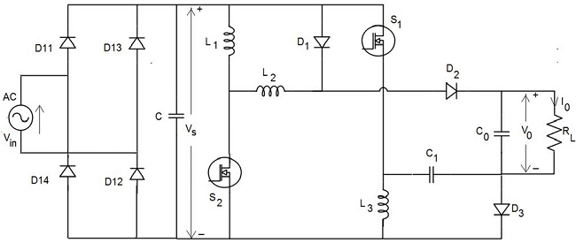
Figure 1
Circuit configuration of the proposed rectifier-fed non-isolated positive output DC-DC boost converter.
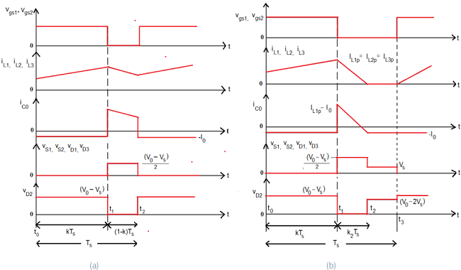
Figure 2
Theoretical waveforms of the converter under study during (a). continuous inductor current mode, and (b). discontinuous inductor current mode.
2.1. Mode-I operation of the converter during the time interval t0-t1
2.1.1. Steady-state analysis:
Both the high power semiconductor switches S1 and S2, of the converter under continuous inductor current mode / discontinuous inductor current mode, are switched on during the time interval . This mode of operation of the converter is represented in Figure 3. The diodes and get forward-biased. The diode gets reverse-biased. The average rectified DC output voltage charges all the three identical inductors in parallel, and the load resistor receives the energy from the capacitor . The diodes and MOSFETs used in this work are assumed as ideal devices having negligible forward voltage drops due to negligible resistance during forward conduction mode. All three inductor currents will be equal since the three inductors are identical and are connected across during mode-I operation as shown in Figure 3. The capacitor also gets charged from the source .
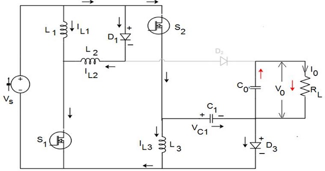
Figure 3
Circuit representation of the converter during Mode-I operation.
Thus, the three identical inductors and the capacitor are charged in parallel to the source voltage Vs .
2.1.2. State-space analysis:
The dynamic and output equations of the circuit for the ON period of the switches S1 and S2 are obtained as follows:
By applying Kirchhoff’s Voltage Law to the circuit shown in Figure 3, we get
Since all the three identical inductors carry equal currents,
Eqn.(2) can be written as:
By applying Kirchhoff’s Current Law to the circuit shown in Figure 3, we get
From Eqns (2.b) and (3.a), the state-space model of the proposed converter during ON period is written as Eqns. (4.a) and (4.b):
2.2. Mode-II operation of the converter during the time interval t1 - t2:
2.2.1 Steady-state analysis:
Both the high power semiconductor switches and , of the converter under continuous inductor current mode / discontinuous inductor current mode, are turned-off during the time interval . This mode of operation of the converter is represented in Figure 4. The diode D2 gets biased in the forward direction. The diodes D1 and D3 get biased in the reverse direction. During mode-I, the diode was forward biased. Therefore, the current flow through will be as shown in Figure 3. Whereas during mode-II, the diode D1 gets reverse biased. Hence, the diode D1 gets open circuited and the diode D2 gets forward biased. Therefore, the current flow through during mode-II in Figure 4 will be opposite to that during mode-I shown in Figure 3. All the three identical inductors and the capacitor are connected in series with the average DC voltage source to transfer the energies to the capacitor and the load resistor . However, the current through the inductors are decreased to zero at the end of the interval () during discontinuous inductor current mode. Under continuous inductor current mode of the converter during mode-II, the voltages across the inductors are obtained as (Yang et al., 2009):
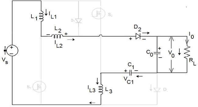
Figure 4
Circuit representation of the converter during Mode-II operation.
From the Figure 4, it is understood that all the three identical inductors carry the same current. Hence, they have the equal voltage drop of Vs across them.
Therefore,
The Inductor Volt-Second Balance (IVSB) principle states that for steady state operation of an inductor in a DC-DC converter, the net inductor voltage in a switching period must be zero. By referring Figure 2, the following Eqn. (7) is obtained by applying the IVSB principle on the inductors L1, L2 and L3:
Finally, the voltage gain under continuous inductor current mode operation of the converter with the active switches having duty ratio is obtained as:
2.2.2. State-space analysis:
The dynamic and output equations of the circuit for the OFF period of the switches and are obtained as follows:
By applying Kirchhoff’s Voltage Law to the circuit shown in Figure 4, we get
By applying Kirchhoff’s Current Law to the circuit shown in Figure 4, we get
From Eqns (9.b) and (10.b), the state-space model of the proposed converter during OFF period is written as Eqns. (11.a) and:
2.3. Mode-III operation of the converter during the time interval t2 - t3:
Both the active switches and of the converter under discontinuous inductor current mode are still switched-off during the time interval . This mode is represented in Figure 5. All the three diodes are not conducting. The three inductors have no stored energy. Thus, the load receives the power delivered by the capacitor C0.
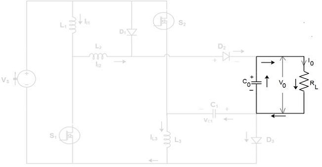
Figure 5
Circuit representation of the converter during Mode-III (Discontinuous inductor current mode) operation.
3. MATLAB / SIMULINK model of the converter under study and its time-domain simulation results
The Simulink model of the rectifier-fed non-isolated positive output converter is developed as shown in Figure 6 and the converter operating under continuous inductor current mode is simulated in Matlab/Simulink environment at a switching frequency of 3 kHz. Table 1 lists the values of circuit components used for simulation. Table 1 also lists the specifications of the converter under study. The converter circuit is simulated using solver ‘ode 45’ of variable-step type. A graphical user interface (GUI) is utilized by the simulink for solving process related simulations. The gating signals given to the active switches and are indicated in Figure 7. The duty ratio ‘’ of the switches is varied between 0.5 and 0.9. But, at extremely low duty ratio itself, high voltage conversion ratio is obtained. The waveforms of input AC voltage, load voltage and load current are indicated in Figure 8 and Figure 9 respectively. The currents through the three identical inductors are shown in Figure 10. The waveforms of voltages across the three inductors are shown in Figure 11. The waveforms of voltages across and the currents through the capacitors and are shown in Figure 12 and Figure 13 respectively. The capacitor has sudden variation of voltage across it due to the change of direction of current through it when the mode of operation changes from I to II. The voltage stresses across the switches are indicated in Figure 14. The waveforms of current through the switches are shown in Figure 15. Figure 16 shows the waveforms of voltages appearing across the diodes . The waveforms of the currents through the diodes are shown in Figure 17. An AC input voltage of 30 V (rms) is given as input to the diode rectifier. At the end of the rectifier, an average DC output voltage of around 90 V is obtained. The output voltage across the load for the duty ratio is almost 900 V (DC), which is almost 10 times the average DC voltage obtained at the output of the rectifier. The load current is of the order of 0.2 A. The active switches are subjected to the voltage stress of around 83 V only. The active switch stresses are reduced as the duty ratio ‘’ of the switches increases.
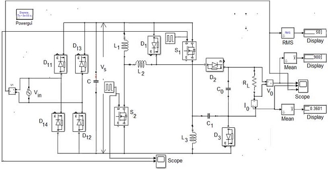
Figure 6
Simulation diagram of the proposed rectifier-fed DC-DC converter configuration
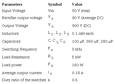
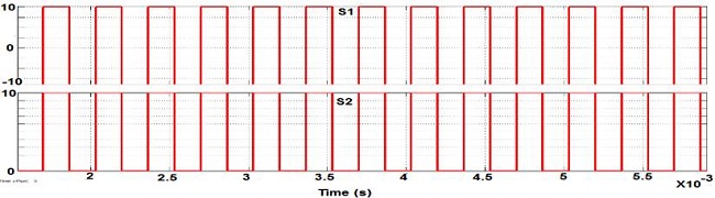
Figure 7
Gating pulses to the switches S1 and S2.
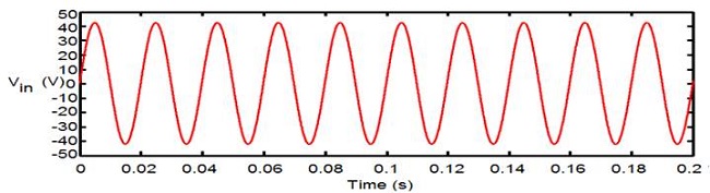
Figure 8
Input AC voltage (Vin) waveform as a function of time.
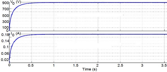
Figure 9
Output voltage and output current waveforms.
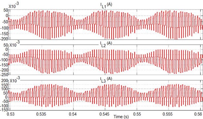
Figure 10
Currents through inductors L1, L2, and L3.
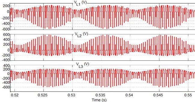
Figure 11
Voltages across the inductors L1, L2, and L3.
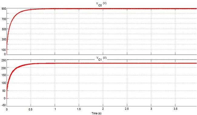
Figure 12
Voltages across the capacitors C0 and C1.
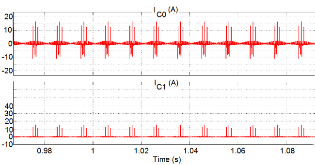
Figure 13
Currents through the capacitors C0 and C1.
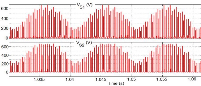
Figure 14
Voltage stresses across the switches S1 and S2.
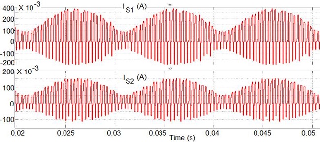
Figure 15
Currents through the switches S1 and S2.
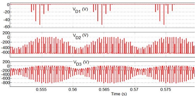
Figure 16
Voltages across the diodes D1, D2, and D3.
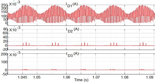
Figure 17
Currents through the diodes D1, D2, and D3.
4. Conclusion
In this article, the open-loop implementation of a rectifier-fed non-isolated positive output high step-up gain power electronic converter has been proposed. The high output voltage level is obtained by a parallel-charge and series-discharge inductor-based voltage boosting technique. The principle of operation and steady state analysis of the proposed converter under continuous inductor current mode operation is analyzed. Both the steady state analysis and state-space analysis of the suggested converter are carried out. The performance of the rectifier-fed DC-DC converter is validated through the time-domain simulations carried out in Matlab/Simulink platform. The results demonstrate that the rectifier-fed converter configuration proposed in this work has the capability to produce an output DC voltage of around 900 V which is almost ten times the average input DC voltage. This improved output voltage level is obtained at extremely low duty ratio of the active switches. The output voltage and output current waveforms are characterized by significantly reduced overshoot and settling time. The voltages across and the currents through the non-dissipative elements in the converter configuration are also analyzed. The proposed converter configuration employs only two high power semiconductor switches (MOSFETs). There is a considerable reduction in the voltage and current stresses for the MOSFETs. The proposed step-up converter may find applications in many real time applications such as battery backup for uninterruptible power supplies, solar cell energy conversion system, automobiles, micro-ovens, and X-ray machines and CT scanners.
References
Adlakha, R., Khosla, A., & Joshi, D. (2020). Comparative analysis of positive output super lift DC-DC luo converters. Indonesian Journal of Electrical Engineering and Computer Science, 18(2), 707-716. https://doi.org/10.11591/ijeecs.v18.i2.pp707-716
Bhaskar, M. S., Kulkarni, R. M., Padmanaban, S., Siano, P., & Blaabjerg, F. (2016). Hybrid non-isolated and non-inverting Nx interleaved DC-DC multilevel boost converter for renewable energy applications. Proceedings of IEEE16thInternational Conference on Environment and Electrical Engineering, IEEE-EEEIC’16, 1-6. https://doi.org/10.1109/EEEIC.2016.7555827
Bhaskar, M. S., Sanjeevikumar, P., Blaabjerg, F., Ojo, O., Seshagiri, S., & Kulkarni, R. (2016). Inverting Nx and 2Nx non-isolated multilevel boost converter for renewable energy applications. Proceedings ofIET International Conference on Clean Energy and Technology, IET-CEAT’16, 1(8.)-1(8.). https://doi.org/10.1049/cp.2016.1258
Chub, A., Vinnikov, D., Blaabjerg, F., & Peng, F. Z. (2016). A review of galvanically isolated impedance-source DC-DC converters. IEEE Transactions on Power Electronics, 31(4), 2808-2828. https://doi.org/10.1109/TPEL.2015.2453128
Dobi, A. M., & Sahid, M. R. (2020). Non-isolated LLC resonant DC-DC converter with balanced rectifying current and stress. Indonesian Journal of Electrical Engineering and Computer Science, 18(2), 707-716. https://doi.org/10.11591/ijeecs.v18.i2.pp698-706
Duarte, J., Lima, L., Oliveira, L., Mezaroba, M., Michels, L., & Rech, C. (2013). Modeling and digital control of a single-stage step-up/down isolated PFC rectifier. IEEE Transactions on Industrial Informatics, 9(2), 1017-1028. https://doi.org/10.1109/TII.2012.2222039
Dwari, S., & Parsa, L. (2011). An efficient high-step-up interleaved dc-dc converter with a common active clamp. IEEE Transactions on Power Electronics, 26(1), 66-78. https://doi.org/10.1109/TPEL.2010.2051816
Evran, F., & Aydemir, M. T. (2014). Isolated high step-up dc-dc converter with low voltage stress. IEEE Transactions on Power Electronics, 29(7), 3591-3603. https://doi.org/10.1109/TPEL.2013.2282813
Forouzesh, M., Siwakoti, Y. P., Gorji, S. A., Blaabjerg, F., & Lehman, B. (2017). Step-up dc-dc converters: a comprehensive review of voltage-boosting techniques, topologies, and applications. IEEE Transactions on Power Electronics, 32(12), 9143-9178. https://doi.org/10.1109/TPEL.2017.2652318
Gautam, D., Sharma, A. K., & Shukla, J. (2019). A review of voltage boosting techniques for step-up DC-DC converter. International Journal of Innovative Research in Electrical, Electronics, Instrumentation and Control Engineering, 7(6), 35-41. https://doi.org/10.17148/ijireeice.2019.7607
He, P., & Khaligh, A. (2017). Comprehensive analyses and comparison of 1 kW isolated DC-DC converters for bidirectional EV charging systems. IEEE Transactions on Transportation Electrification, 3(1), 147-156. https://doi.org/10.1109/TTE.2016.2630927
Hossain, M. Z., Selvaraj, J. A. L., & Rahim, N. A. (2018). High voltage-gain full-bridge cascaded dc-dc converter for photovoltaic application. PLOS ONE, 13(11), 1-21. https://doi.org/10.1371/journal.pone.0206691
Hsieh, Y. P., Chen, J. F., Liang, T. J., & Yang, L. S. (2012). Novel high step-up DC-DC converter with coupled inductor and switched-capacitor techniques. IEEE Transactions on Industrial Electronics, 59(2), 998-1007. https://doi.org/10.1109/TIE.2011.2151828
Hu, X., & Gong, C. (2014). A high voltage gain DC-DC converter integrating coupled-inductor and diode-capacitor techniques. IEEE Transactions on Power Electronics, 29(2), 789-800. https://doi.org/10.1109/TPEL.2013.2257870
Li, W., & He, X. (2011). Review of nonisolated high-step-up dc/dc converters in photovoltaic grid-connected applications. IEEE Transactions on Industrial Electronics, 58(4), 1239-1250. https://doi.org/10.1109/TIE.2010.2049715
Mahajan, S. B., Sanjeevikumar, P., & Blaabjerg, F. (2017). Multistage DC-DC step-up self-balanced and magnetic component free converter for photovoltaic applications-hardware implementation. Energies Journal, 10(5), 1-28. https://doi.org/10.3390/en10050719
Mahajan, S. B., Sanjeevikumar, P., Ojo, O., Rivera, M., & Kulkarni, R. (2016). Non-isolated and inverting Nx multilevel boost converter for photovoltaic DC link applications. Proceedings ofIEEE International Conference on Automatica IEEE-ICA-ACCA’16, 1-8. https://doi.org/10.1109/ICA-ACCA.2016.7778453
Nguyen, M. K., & Chai, Y. O. (2019). Voltage multiplier-cell based quasi-switched boost inverter with low input current ripple. Electronics, 8(227), 1-18. https://doi.org/10.3390/electronics8020227
O’Loughlin, O. (2006). An interleaving PFC pre-regulator for high-power converters, Texas Instruments, 1-14.
Prabhala, V. A. K., Fajri, P., Gouribhatla, V. S. P., Baddipadiga, B. P., & Ferdowsi, M. (2016). A dc-dc converter with high voltage gain and two input boost stages. IEEE Transactions on Power Electronics, 31(6), 4206-4215. https://doi.org/10.1109/TPEL.2015.2476377
Qian, W., Cao, D., Cintron-Rivera, J. G., Gebben, M., Wey, D., & Peng, F. Z. (2012). A switched-capacitor DC-DC converter with high voltage gain and reduced component rating and count. IEEE Transactions on Industrial Applications, 48(4), 1397-1406. https://doi.org/10.1109/TIA.2012.2199731
Rosas-Caro, J. C., Mayo-Maldonado, J. C., Salas-Cabrera, R., Gonzalez-Rodriguez, A., Salas-Cabrera, E. N., & Castillo-Ibarra, R. (2011). A family of dc-dc multiplier converters. Engineering Letters, 19(1), 57-67.
Roy, J., & Ayyanar, R. (2017). Sensor-less current sharing over wide operating range for extended-duty-ratio boost converter. IEEE Transactions on Power Electronics, 32(11), 8763-8777. https://doi.org/10.1109/TPEL.2016.2640319
Saravanan, S., & Ramesh Babu, N. (2019). A modified high step-up non-isolated DC-DC converter for PV application. Journal of Applied Research and Technology, 15(3), 242-249.https://doi.org/10.1016/j.jart.2016.12.008
Tofoli, F. L., de Castro Pereira, D., de Paula, W. J., & Júnior, D. D. S. O. (2015). Survey on non-isolated high-voltage step-up dc-dc topologies based on the boost converter. IET Power Electronics, 8(10), 2044-2057. https://doi.org/10.1049/iet-pel.2014.0605
Tseng, K. C., & Huang, C. C. (2014). High step-up, high efficiency interleaved converter with voltage multiplier module for renewable energy system. IEEE Transactions on Industrial Electronics, 61(3), 1311-1319. https://doi.org/10.1109/TIE.2013.2261036
Wai, R. J., Lin, C. Y., Duan, R. Y., & Chang, Y. R. (2007). High-efficiency dc-dc converter with high voltage gain and reduced switch stress. IEEE Transactions on Industrial Electronics, 54(1), 354-364. https://doi.org/10.1109/TIE.2006.888794
Wu, T. F., Chen, Y. C., Yang, J. G., & Kuo, C. L. (2010). Isolated bidirectional full-bridge dc-dc converter with a flyback snubber. IEEE Transactions on Power Electronics, 25(7), 1915-1922. https://doi.org/10.1109/TPEL.2010.2043542
Yang, L. S., Liang, T. J., & Chen, J. F. (2009). Transformer-less DC-DC converter with high voltage gain. IEEE Transactions on Industrial Electronics, 56(8), 3144-3152. https://doi.org/10.1109/TIE.2009.2022512
Yaramasu, V., & Wu, B. (2011). Three-level boost converter based medium voltage megawatt PMSG wind energy conversion systems. Energy Conversion Congress and Exposition (ECCE), 561-567. https://doi.org/10.1109/ECCE.2011.6063819
Notes
Author notes
∗ Corresponding author. E-mail address: muraliems@gmail.com(D. Murali).