VHDL Optimized Model of a Multiplier in Finite Fields1
Modelo VHDL optimizado de un multiplicador en campos finitos2
VHDL Optimized Model of a Multiplier in Finite Fields1
Ingeniería y Universidad, vol. 21, no. 2, 2017
Pontificia Universidad Javeriana
Received: 26 June 2016
Accepted: 19 May 2017
Abstract: Introduction: This article presents a finite field multiplier (GF) model, studying the generalized architecture of the LFSR component (linear regression displacement records), in order to generate a concurrent description. Concepts of structural analysis, description of parameterized components, and mathematical treatment of signals have been applied. Method: The design was performed by the tabulation of the terms in the variable time function and the position in the circuit, the components of the modular reduction, thus creating an array of combined operations. This model was described in VHDL, for testing behavior and optimization of hardware. Results: The research established the equations for the implementation of the VHDL model in its generic expression with operator concatenation for the hardware configuration. It is estimated that the hardware resources, a level of logical operators, obtained a 7.89% savings in the energy consumption associated with the signal in the multiplier design by the proposed optimization technique. Conclusions: The model simplified the description of parallel circuits, high performance from a mathematical model approach to hardware description. The proposed method contributes to the field of optimization in the efficient modeling of advanced logic systems, which can be extrapolated to more complex components.
Keywords: VHDL model, Finite FieldsMultiplier, circuital optimization.
Resumen: Introducción; Este artículo presenta el modelo de un multiplicador en campos finito GF, estudiando la arquitectura generalizada del componente LFSR (registros desplazamientos con realimentación lineal), esto con el propósito de generar una descripción concurrente. Se han aplicado conceptos de análisis estructural, descripción de componentes parametrizados, tratamiento matemático de señales. Método: EL diseño se realizó a través de la tabulación de los términos en función de las variables tiempo y posición en el circuito, del componente de reducción modular, creando así una matriz de operaciones combinacionales, este modelo fue descrito en VHDL, para las pruebas de comportamiento y optimización del hardware. Resultados: La investigación permitió establecer las ecuaciones para la implementación del modelo en VHDL, en su expresión genérica con el operador “concatenación, para la configuración de hardware, se estimó el consumo de recursos hardware, a nivel de operadores lógicos, obteniéndose una propuesta eficiente. Así mismo, se obtiene un 7.89% de ahorro del consumo de potencia asociada a la señal en el diseño del multiplicador, con la técnica de optimización propuesta. Conclusiones: El modelo desarrollado simplifica la descripción de circuitos paralelos, de alta eficiencia desde un enfoque de modelado matemático para descripción de hardware. El método propuesto muestra sus aportes en materia de optimización en el modelado eficiente de sistemas lógicos avanzados, el cual puede ser extrapolado a componentes más complejos.
Palabras clave: Modelo VHDL, Multiplicador en campos finitos, optimización circuital.
1. Introduction
Study of the RS coder [1] for efficient implementation found that they use Galois GF (2m) finite field arithmetic to produce fixed length results and that their operations can be implemented with relatively simple circuitry [2]. Some of these operations are more complex, which led researchers to focus on the optimization of multiplication algorithms [3]. It should be borne in mind that the computational efficiency of arithmetic operations in finite fields is closely related to the particular way in which field elements are presented [4]. Therefore, we have detected the need to study solution alternatives for the implementation of GF arithmetic operations (2m) based on the mathematical foundations of finite fields.
The Finite Fields of Galois constitute a specific area of mathematics developed by E. Galois. The field is specified by a prime element p (base of the field) and a positive integer m, length of the field element; pm corresponds to the number of elements of the field, and the arithmetic operations on the finite field result in an element that belongs to the same [5]. These properties are used in applications of coding, Reed-Solomon decoding [6] and cryptography. A widely used presentation is the polynomial form, in which a field-generating polynomial, known as an irreducible polynomial p(x), is defined that will operate with the results of operations to bring the result to the fixed length defined for field.
A model that is configurable in a device that supports concurrent implementation that allows incorporation of Reed Solomon encoders is proposed. These multipliers are basic components that require implementation in a highly efficient way for speed and consumption of resources and power by the fractal nature of these circuits [7] and the concatenation of complex codes [8].
2. Finete field multiplicators
The multiplier in finite fields is generally more complex than a conventional multiplier [9]. These have been a topic of investigation; therefore, the relevance of interpreting the circuit support logic for these modules and establishing an efficient model for their design on FPGA hardware. The arithmetic multipliers of Galois finite fields are based on the multiplication of two elements of the finite body and the reduction of the result by an irreducible polynomial p(x) of degree m. These can be implemented by an algorithmic model, which reproduces the behavior of the multiplier sequentially [10] or with parallel models, depending on the need for these arithmetic modules to operate at high frequencies and occupy the smallest possible area, which demands a balance between these factors. This commitment has led to the search for efficient algorithms and architectures, as indicated by research in the area [11].
Among the models available, the multiplier proposed by Karatsuba-Ofman [12] consists of a modular sub-division technique of the multiplier component, combinational models [13], through tables [14] and table-algorithm combinations [15]. The latter presents a contribution in reducing resources based on the original implementation of 255x255 tables, equivalent to 65025 8-bit symbols, to 256 8-bit symbols for the multiplier; however, this reduction still demands 512 LUTs of 4 inputs when making the expansion to cover the table.
At the level of optimization of implementations are the Mastrovito Multiplier (combinational - matrix), Massey-Omura Multiplier, Hasan-Bhargava Multiplier, Paar-Rosner Multiplier, Morii-Berlekamp Multiplier, Pipelined Combinational Multiplier, Linear Feedback Shift Multiplier - LFSR all these are described in [16]. Additionally, to achieve scalability, several algorithms have been proposed, all implemented in hardware [17].
From the study of previously developed GF multiplier models, the GF (16) Mastrovito, Paar-Rosner and Pipelined Combinatorial multipliers were found to have the lowest consumption and highest speed compared to alternative multipliers. For this reason, they have been considered as reference for the evaluation of the results, although some of these multipliers present optimization for a particular approach to the architecture and have been an important contribution for the interpretation of optimization alternatives. From the models studied, the LFSR-based multiplier is considered as the base for the optimization. It presents a latency of m clock pulses, which can be parallelized under a temporal analysis of the circuit.
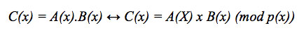
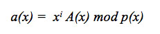
This analysis is based on the study of the mathematical model of polynomial representation, in which it is stated: If p(x) is the irreducible polynomial, then the multiplication of two elements of the field, represented as the polynomials A(x) and B(x) is the algebraic product of the two polynomials, and the modulus operation of the polynomial p(x), also known as modular reduction, is that shown in equation 1.
 [equation 1]
The multiplication of polynomials is associative, commutative and distributive with respect to the addiction whereby we obtain equation 2.
 [equation 2]
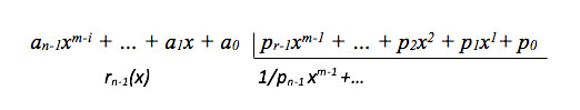
where A(x) and B(x) correspond to the polynomial representation of the operands. In the case of the RS encoder, the multiplicand A(x) corresponds to a coefficient of the code generator polynomial, the multiplier B(x) to the data input, and p(x) is the irreducible polynomial of the Galois field. For the calculation of the modular reduction, the concept of the division of polynomials on finite fields is used, whose mathematical expression is presented in equation 3.
 [equation 3]
where r(x) = A(x) mod p(x) corresponds to the remainder of the division between the operand A(x) of the multiplication and the irreducible polynomial of the finite field GF(2m). For the circuital implementation of the equations, the stages of the multiplier in finite fields must be identified. First, the model proposed by [9], which includes a modular reduction step in the results, is divided into four levels of operation on the data. In Figure 1, the stages are presented based on the initial model, where the m-bit operands and the displacement of the partial products that give rise to an accumulation of length m+m-1 are observed, which generates a resultant element that does not belong to the finite field and a conversion must be incorporated through a final reduction so that the product corresponds to an element of the field.
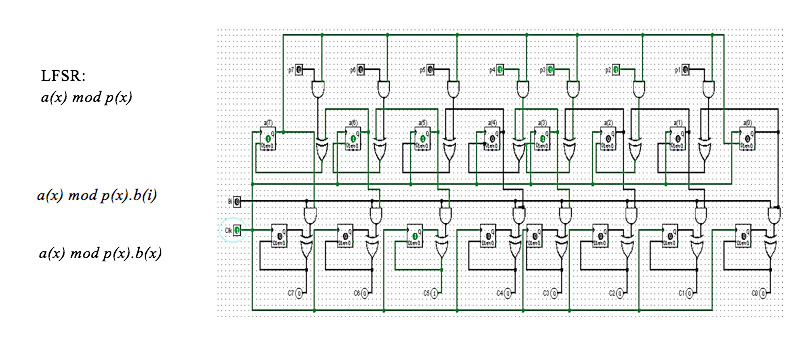
Figure 1
Circuit diagram of GF (2m) Multiplier
Source: Author’s own elaboration
The circuit diagram of the multiplier GF(2m) comprises three stages: the operation circuit module p(x) implemented by an LFSR circuit, obtaining the modular reduction of the polynomial A(x), the partial product module with the element Bi implemented by a set of parallel AND gates. The accumulator of partial products, implemented by XOR gates in case of being sequential are fed back using flip-flop memory storage devices. The case of the polynomial generator of the finite field is P(x) = x8+ x4+ x3+ x2+ 1.
The architecture of the modular reduction stage is based on generators of Galois sequences; its properties are studied in [18]. From there it is observed that it was originally implemented by registers to obtain the n vectors corresponding to the partial residues. This is by means of bit shift over the structure in m clock cycles, where m is equal to the number of bits of the word, in the case of a GF field (28), with 256 field elements of 8 bits in length. The model of a configurable LFSR is of great interest for the synthesis process [19]. Based on this, we propose the analysis of the behavior of the temporal results generated by the LFSR structure in order to construct a mathematical model, oriented to the description in VHDL.
From the circuit model and the construction of terms as a function of the instant and the spatial position, the behavior of the polynomial divisor module is determined to obtain the vectors a1 ... a8, the result of A(x) mod p(X) using concatenation instead of sequential processing. The implementation is reduced to the use of AND gates between each coefficient of p(x), and the use of XOR gates that operate with partial coefficients results, all in the same clock pulse. In this way, the configuration syntax for a parallelized version of this multiplier in VHDL is created where the sequential components have been eliminated and replaced by variables that depend on combinational functions.
Starting from the analysis of multiplier architectures [20], we can observe a combinational multiplication step composed of a set of ANDs and XORs and a sequential modular reduction step, which implements a division of polynomials between a finite field element A(x) ∈ GF and the irreducible polynomial that defines the field p(x). If it is possible to define the LFSR model through a concurrent implementation [21], the area and power consumed are similar and even less compared to the sequential version [22]. For this, we analyzed optimizations on the circuit [18] and a mathematical model for the generation of the sub-sequences, considering that applications of high performance require parallel implementations [23].
3. Method of description of multiplicate GF in VHDL
The modules for data processing in finite field algebra GF(2m) can be programmed in software, through algorithms for sequential processing or hardware solutions for concurrent models, the latter being the model that is proposed. An alternative for the implementation of this model is based on search tables, allowing changing the representation of the elements of the field GF (2m), or through a circuit model where the design of the module is based on the mathematical model and behavior interpretation of the circuit. For this purpose, the architecture was analyzed, using modular reduction based on the LFSR.
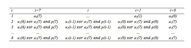
For the interpretation and analysis of the LFSR device with sequential structure, we proceeded to describe each sequence generated at an instant of time t, thus obtaining the associated states, and the mathematical representation of the sequential LFSR. At this point, we proceeded to describe the behavior of the circuit for each clock pulse, using the position indexes corresponding to each memory element and the logical operations that are performed for the construction of the terms for which the description are given in Table 1.
Source: Author’s own elaboration
From the description in VHDL, it is possible to reproduce the LFSR in parallel. These data allow us to generalize the equations. At time t = 1 the resulting vector will be the data input, D_date, at time t = 2 we have the partial vector of the circuit operation, shown in equation 4.
 [equation 4]
where operations are defined by the AND and XOR logic operations because the operands are binary elements, corresponding to the coefficients of the polynomials A(x) and p(x). An analysis of the time outputs of the circuit during its operation yields an array of equations, which depend on the clock cycle and the position of the vector and allow the calculation of the terms generated by the LFSR circuit. The mathematical-logical relationship for each of the elements generated by the LFSR component are presented in Table 2, as an array of combinational operations, that describes the parallel multiplier model.
Source: Author’s own elaboration
In this table we can observe the relationship of the terms when applying the operation of each branch of the LFSR circuit on the polynomial A(x). Each branch is represented by the coefficient of the generator polynomial of the field p(x) in position i, corresponding to p(i), which will be fixed in time. Since the modular reduction operation generates a set of m partial residues, according to which its behavior can be described, it is proposed to parameterize the generating function of each element. In this way, the method used is association of the sub-indices with the relation of the parameters given by the position i and the time instant t.
Based on this modeling technique we establish the coefficients of the residual polynomial as a function of time as at(i); the coefficient of the polynomial in the most significant position as at-1(m-1), representing the most significant bit fed back into the circuit, at a time instant t-1 and at-1(i-1), which corresponds to the preceding bit of the calculated element. From this procedure the equations were developed that describe the behavior of the LFSR circuit for its parallel description, in order to achieve the implementation of the concurrent structure for VHDL.
Hardware Description Optimization Techniques
The simplification of the circuit is proposed, defining this as a function of the characteristic polynomial. The first step is the selection of the irreducible or primitive polynomial for the generation of the field; these polynomials are characteristic of the length m of the field GF (2m) and are presented in detail in [24]. The criterion that must be met is that they divide the elements of the finite field and cannot be written as the product of two field polynomials [25].
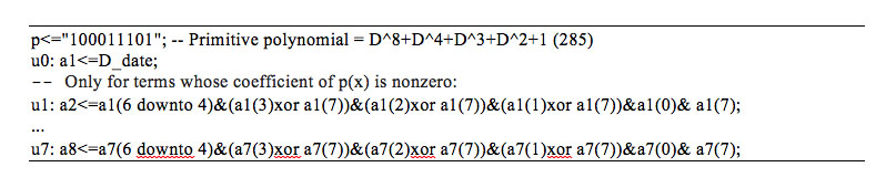
A polynomial satisfying such a condition is the polynomial p(x) = 285, which has been selected because it is a polynomial GF field generator widely used in standard RS encoders [26]. At this point the steps of the calculation of the multiplication in finite fields were studied to describe them concurrently in VHDL language in order to obtain the model for the hardware implementation of the multiplier. Using the polynomial generator of the field in its binary form, p(x) = 100011101, which is a polynomial of degree m = 8, we obtain the particularized model shown in Figure 2.
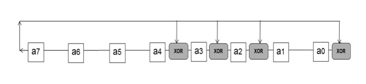
Figure 2.
LFSR model for p(x) = 285
Source: Author’s own elaboration
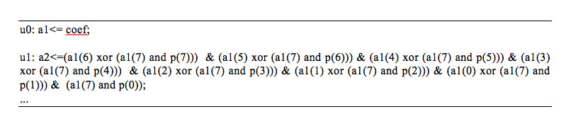
This simplified circuit of the modular reduction component presents a saving in the resource consumption of the device. The VHDL description of the concurrent LFSR circuit model used by the multiplier is generated from a simplification of Table 2 by the direct cancellation of the branches whose coefficients are “0” in the selected irreducible polynomial, resulting in the VHDL code of the simplified structure, presented in Table 3.
Source: Author’s own elaboration
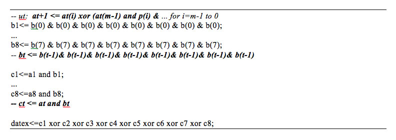
The products must be implemented with AND gates between the elements of the partial outputs of the LFSR, which are at, i, a vector of m elements, with the data element bt, the bit being in the position t of the input B. In bitwise parallel, in order to obtain the resulting vectors by ci, j, corresponding directly to at, i, in case the bit in the respective position of bt is equal to ‘1’, in case otherwise it will be annulled. A vector Bt is defined as the concatenation of the element bt, m times, the partial results operate through XOR gates for the results of the final product, as described in Table 4.
Source: Author’s own elaboration
4. Results
The test benches of the components were created to observe the response of the designed modules. To validate the GF multiplier, based on LFSR, we considered the parameter m = 8, with a field generator polynomial p(x) = 285, and the coefficients 104 and 13. The multiplication of the first 16 elements of the finite field GF (256), generated the expected results, in parallel (see Figure 3).
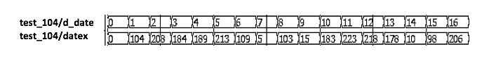
Figure 3a
Multiplication on GF (256) with coefficient 104
Source: Authors' own elaboration
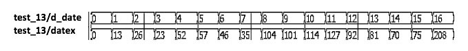
Figure 3b
Multiplication on GF (256) with coefficient 13
Source: Authors' own elaboration
The operation of the RS encoder (255, k) was validated for the cases studied when the multiplier components to be used in the encoder were tested. For this purpose, the parameter k variable was established, which was assigned the values 223, 239 and 247 , using the polynomial generator of RS code for each case. The coefficients of the polynomial G(x) are assigned in the step of the encoder redundancy generator. For its operation with the data D(x), the data entry uses values from 1 to k increasing, set in the test_bench. In each case, the 255-k corresponding redundancy symbols are obtained. The simulation was performed using the ModelSim XE III 6.3c tool, incorporated in the ISE of Xilinx. The coded word generated corresponded with the result expected from the theoretical behavior.At the resource level of the FPGA hardware device a logical complexity of 3 stages is obtained (modular reduction), demonstrating that the depth of the design does not interfere in the propagation speed of the signals, as shown in Figure 4.
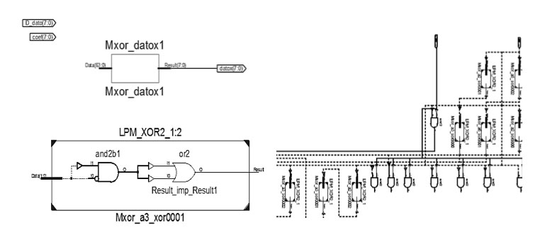
Figure 4
Schematic of the concurrent multiplier GF (2m)
ource: Author’s own elaboration
To implement the circuit, 44 reported LUTs were required, the Slice number is associated with the number of LUTs of the FPGA as mentioned before, the device XC5VLX30 presents 4 LUTs per Slice. The number of inputs required by LUTs for the design is 6, 4 and 3, requiring 17 Slices, as shown in Table 5, which is a significant reduction of FPGA components, compared to previous reports.
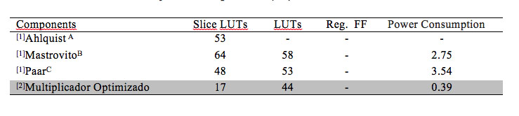
Source: [1] Comparative Table [27]; [2] Dynamic Power Consumption supplied by the XPower of the ISE11 in mW for the FPGA XC5VLX30 [28].
OPTIMIZATION FOR SIGNAL ALLOCATION
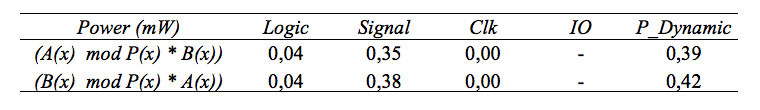
After the theoretical analysis, the power consumption in mW of the designed modules was obtained, using Xilinx’s XPower Analyzer tool, as shown in Table 6, considering as a comparison factor the order of allocation of the signals for the multiplier circuit [29].
Source: Author’s own elaboration
The power consumption associated with the logic of the P_Logic circuit in both cases was 0.04 mW, while the P_Signal presented a variation according to the order of the operands, consuming a power associated with the signals of 0.38 mW. In the case of B(x) mod p(x). A(x), a power consumption of 0.35 mW; in the case of A(x) mod p(x). B(x), this optimization was achieved through the signal reordering technique; in this case the results of the multiplier were tested using the commutative property of the operations. There is no consumption associated with the clock signal P_clk, since the multiplier is concurrent and there is no consumption of P_IO because it is an internal component and the signals of the multiplier are not implemented in the external pins of the FPGA. The order of the inputs was found to only have an effect on the P_Signal that corresponds to a technique of decrease of the consumption that will be used for the design of the modules of the encoder. Based on the power ratio of the optimized design and the original version, a 7.89% savings in the power consumption associated with the signal in the multiplier design was obtained.
The model was developed starting from the expression of the polynomials generated as partial residues in the multiplication operation in finite fields, which was expressed as a function of the xi displacements in the multiplication operation with the corresponding Bi coefficient.
 [equation 5]
The matrix expression for the product of symbols in Galois finite fields can be expressed as:
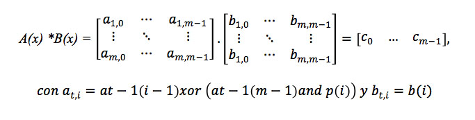 [equation 6]
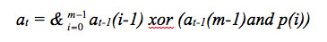
After obtaining the multiplier equations in VHDL, a mathematical-logical model for reconfigurable hardware was obtained from the study of the equations of each of the elements of the LFSR presented in Table 2. In this way, a generalization of the behavior of the elements at(i) was obtained in equation 7.
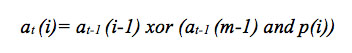 [equation 7]
at is an element generated at a time t to apply the modular reduction, A(x) mod p(x), resulting from the operation and between p(i), the polynomial coefficient of the feedback function at position i , with the element at-1 in the most significant position of the previous symbol, this term XOR with at-1, in position i. It is important to note that the optimization by signal organization has been considered, in which the order of multiplication factors affects the efficiency of the design, the most efficient distribution of signals being presented in the model.
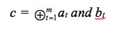
Next, the general equation of the residual vector of the modular division or reduction was defined for each time instant, using the variable t as an operation reference with the elements of B(x). Using the concatenation operation, substitute the clock signal to generate the sequence of the bits given by equation 7, from which equation 8 is obtained.
 [equation 8]
Where the ‘&’ symbol is used to indicate the concatenation operation in order to match the description in VHDL. This is optimized by parallelizing the circuit by concatenation of signals for concurrent processing. To implement the combinational step of the product of A(x) xi mod p(x).B(x), which corresponds to the AND operation of each element of B(x) for each at and the summation XOR of these, equation 9 is derived.
 [equation 9]
Substituting equation 8 into equation 9, gives the model of the multiplier as equation 10.
 [equation 10]
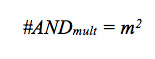
This equation has the variable i for nonzero coefficients of the polynomial p(x), which achieves an optimization by the simplification of the equations, as mentioned in the efficiency analysis. This VHDL model allows the resource consumption analysis based on the multiplier architecture, which has been parallelized through the concurrent description of the modular reduction stage. This represents an important advance in the proposed multiplier model with the concurrent LFSR component. The calculation of the consumption of gates was established by equation 11, for the calculation of AND required.
 [equation 11]
And for the calculation of consumption of XOR gates we used equation 12
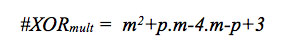 [equation 12]
where m corresponds to the number of bits of each field word and p corresponds to the number of non-zero bits of the irreducible polynomial p(x); in this case the optimization corresponds to the simplification of operations, as a function of the number of coefficients p(x). When analyzing the structure of the VHDL model, the associated direct operands are obtained and an estimation of hardware resources can be made at the level of gates.
CONCLUSION
A model of the studied circuit was found where the description in VHDL was defined for the behavior of the LFSR function, recognizing function generating terms, which maintain relation with the temporal sequence, modeled concurrently. This proposal is innovative because it considers the temporary displacements as concurrent concatenation operations of elements of the circuit, thus optimizing the processing speed and minimum energy consumption, of great interest at the moment. In this way, a model for implementation in hardware is achieved, with updated and highly efficient technology, useful for other developments that reuse GF multipliers as basic elements.
From the model, a generalized hardware description is obtained as a novel contribution since a model has not been found that allows the reproduction of results from a set of basic equations and obtains the results discussed here. This allows dynamic adjustment with great flexibility in its configuration; the adaptive proposal supports hardware development from the parameterized equations and manages to reuse the components, oriented to concurrent implementation, giving a new approach to the design. Similarly, the behavioral principles of the logical systems are the basis for design and optimization, recognizing the associated patterns, in order to achieve the design of a descriptive model at the mathematical - logical level for the generation of the configuration code.
Considering the algorithmic relationship of the hardware functions, it has been proposed to advance this method of modeling, for the optimization of the VHDL designs, with parallel processing capacity, using the least number of resources of the FPGA devices, and tested with a selected study case. We obtained the equations, which describe the GF multiplier, with adaptable parameters, since it was determined that the parameters once assigned allow optimizing the design because the results will be given in a function of the coefficients that defines the characteristic polynomial of the circuit. This is achieved by a highly efficient design and a novel model, which provides a method of hardware configuration, taking advantage of the correspondence with the VHDL code of the components of the multiplier element, for adaptation to new designs.
References
[1] C. Sandoval-Ruiz and A. Fedón-Rovira, “Efficient RS (255 ,k) encoder over reconfigurable systems,” Rev.Téc.Ing.Zulia, vol. 37, no. 2, pp. 151–159, 2014.
[2] R. H. Morelos-Zaragoza, The art of error correcting coding, vol. 2. England: Wiley, 2002.
[3] F. J. Brotons M, “Modelo de Criptoprocesador de Curvas Elípticas en GF(2m) Basado en Hardware Reconfigurable,” Tesis Doctoral, Universidad de Alicante, España, 2016.
[4] C. H. Kim, S. Oh, and J. Lim, “A new hardware architecture for operations in GF(2m),” Comput. IEEE Trans., vol. 51, no. 1, pp. 90–92, 2002.
[5] A. Saqib Nazar, “Implementación Eficiente de Algoritmos Criptográficos en Dispositivos de Hardware Reconfigurable,” Centro de Investigación y Estudios Avanzados del Instituto Politécnico Nacional, México, 2004.
[6] C. E. Sandoval-Ruiz and A. Fedón-Rovira, “Codificador RS (255,k) en hardware reconfigurable orientado a radio cognitivo,” Ing. y Univ., vol. 17, no. 1, pp. 77–91, 2013.
[7] C. Sandoval-Ruiz, “Analysis of Fractal Circuits and Modeling through Iterated Functions System for VHDL Case Study : Reed Solomon Encode,” Rev. Cienc. e Ing., vol. 38, no. 1, pp. 3–16, 2017.
[8] C. E. Sandoval-ruiz, “Logical-Mathematical Model of Encoder 2D-RS for Hardware Description in VHDL,” Rev. Ing. UC, vol. 24, no. 1, pp. 28–39, 2017.
[9] V. C. Tejeda-calderón, M. A. García-martínez, and R. Posada-gómez, “IMPLEMENTACIÓN EN FPGA DE UN MULTIPLICADOR POR DIGITOS SOBRE CAMPOS FINITOS GF ( 2 m ) División de Estudios de Postgrado Orizaba , Veracruz,” pp. 2–5.
[10] J. Cruz, “Multiplicación Escalar en Curvas de Koblitz: Arquitectura en Hardware Reconfigurable,” Instituto Técnico Nacional, 2005.
[11] J. Imaña, “Aplicación de Campos de Galois a la verificación probabilistica de Funciones Booleanas y Métodos de Multiplicación sobre campos de Extensión GF(2m),” Universidad Complutense de Madrid, 2004.
[12] M. Machhout, M. Zeghid, W. El, B. Bouallegue, A. Baganne, and R. Tourki, “Efficient Large Numbers Karatsuba-Ofman Multiplier Designs for Embedded Systems,” Comput. Eng., pp. 548–557, 2009.
[13] G. C. Ahlquist, B. E. Nelson, and M. D. Rice, “Synthesis of small and fast finite field multipliers for field programmable gate arrays,” 2002.
[14] M. Song, S. Kuo, and I. Lan, “A Low Complexity Design of Reed Solomon Code Algorithm for Advanced RAID System,” IEEE Trans. Consum. Electron., vol. 53, no. 2, pp. 265–273, 2007.
[15] G. M. Marchesan Almeida, E. A. Bezerra, L. V. Cargnini, R. D. R. Fagundes, and D. G. Mesquita, “A Reed-Solomon algorithm for FPGA area optimization in space applications,” in Adaptive Hardware and Systems, 2007. AHS 2007. Second NASA/ESA Conference on, 2007, pp. 243–249.
[16] G. Ahlquist, B. Nelson, and M. Rice, “Optimal finite field multipliers for FPGAs,” in Field Programmable Logic and Applications, 1999, pp. 51–60.
[17] J. J. Climent, F. G. Crespí, and A. Grediaga, “A Scalable Finite Field Multiplier,” IEEE Lat. Am. Trans., vol. 6, no. 7, pp. 632–637, 2008.
[18] E. Dubrova, M. Teslenko, and H. Tenhunen, “On Analysis and Synthesis of (n,k) -Non-Linear Feedback Shift Registers,” in Transition, 2008, pp. 1286–1291.
[19] C. I. H. Chen, “Synthesis of configurable linear feedback shifter registers for detecting random-pattern-resistant faults,” in Proceedings of the 14th international symposium on Systems synthesis, 2001, vol. 1, no. V, pp. 203–208.
[20] M. García-Martínez, G. Morales-Luna, and F. Rodríguez-Henríquez, “Implementación En FPGA de un Multiplicador Eficiente para Campos Finitos GF(2m).”
[21] C. Sandoval-Ruiz, “Codificador RS (n,k) basado en LFCS : caso de estudio RS (7,3),” Rev. Fac. Ing. Univ. Antioquia, no. 64, pp. 68–78, 2012.
[22] H. Yap, K. Khoo, and A. Poschmann, “Parallelizing the Camellia and SMS4 Block Ciphers - Extended Version,” 2010.
[23] C. Mucci et al., “Implementation of parallel LFSR-based applications on an adaptive DSP featuring a pipelined configurable Gate Array,” in Design, Automation and Test in Europe, 2008. DATE’08, 2008, no. 27342, pp. 1444–1449.
[24] O. Delgado, “Nuevos Protocolos y Esquemas de Seguridad para Redes Ad-hoc Móviles Inalámbricas, Tesis Doctoral,” Universidad Carlos III de Madrid, 2010.
[25] F. Peralta, “Diseño De Arquitecturas Digitales para Criptografía,” Instituto Politécnico Nacional, 2005.
[26] Xilinx, “LogiCORE IP Reed-Solomon Encoder v8.0,” 2012.
[27] J. D. Allen, “Energy Efficient Adaptive Reed-Solomon Decoding System,” University of Massachusetts Amherst, USA, 2008.
[28] C. Sandoval-Ruiz, “Modelo Optimizado del Codificador Reed-Solomon (255,k) en VHDL a través de un LFSR paralelizado,” Tesis Doctoral, Universidad de Carabobo, Venezuela, 2013.
[29] C. Sandoval Ruiz, “Power Consumption Optimization in Reed Solomon Encoders over FPGA,” Lat. Am. Appl. Res., vol. 44, no. 1, pp. 81–85, 2014.
Notes
Author notes