Artículos
A Novel CMOS reconfigurable rectifier for wearable piezoelectric energy harvesters
Un nuevo rectificador reconfigurable CMOS para recolectores de energía piezoeléctrica en dispositivos portables

A Novel CMOS reconfigurable rectifier for wearable piezoelectric energy harvesters
Revista UIS ingenierías, vol. 21, no. 1, pp. 103-112, 2022
Universidad Industrial de Santander
Received: 09 July 2021
Accepted: 14 September 2021
Abstract: Wearable energy harvesters have potential application in the conversion of human-motion energy into electrical energy to power smart health-monitoring devices, the textile industry, smartwatches, and glasses. These energy harvesters require optimal rectifier circuits that maximize their charging efficiencies. In this study, we present the design of a novel complementary metal-oxide semiconductor (CMOS) reconfigurable rectifier for wearable piezoelectric energy harvesters that can increase their charging efficiencies. The designed rectifier is based on standard 0.18 μn CMOS process technology considering a geometrical pattern with a total silicon area of 54.765 μn x 86.355 μn The proposed rectifier circuit has two transmission gates (TG) that are composed of four rectifier transistors with a charge of 45 kΩ, a minimum input voltage of 500 mV and a maximum voltage of 3.3 V. Results of numerical simulations of the rectifier performance indicate a voltage conversion efficiency of 99.4% and a power conversion efficiency up to 63.3%. The proposed rectifier can be used to increase the charging efficiency of wearable piezoelectric energy harvesters.
Keywords: Complementary Metal Oxide Semiconductor (CMOS) technology, energy conversion, energy harvesters, health monitoring devices, piezoelectric transducer, portable devices, power conversion efficiency, reconfigurable rectifier, transmission gate (TG), voltage conversion efficiency.
Resumen: Los recolectores de energía para dispositivos portables tienen una aplicación potencial en la conversión de la energía del movimiento humano en energía eléctrica para alimentar dispositivos inteligentes de monitoreo de la salud, de la industria textil, así como de relojes y lentes inteligentes. Estos recolectores de energía requieren circuitos rectificadores óptimos que maximicen sus eficiencias de carga. En este estudio se presenta el diseño de un novedoso rectificador reconfigurable metal óxido semiconductor complementario (CMOS) para recolectores de energía piezoeléctrica portables que puede aumentar sus eficiencias de carga. El rectificador diseñado se basa en la tecnología de proceso CMOS estándar de 0,18 um considerando un patrón geométrico con un área total de silicio de 54.765 μm x 86.355 μm. El circuito rectificador propuesto tiene dos puertas de transmisión (TG) que están compuestas por cuatro transistores rectificadores con una carga de 45 kΩ, un voltaje mínimo de entrada de 500 mV y un voltaje máximo de 3,3 V. Los resultados de las simulaciones numéricas del funcionamiento del rectificador indican una eficiencia de conversión de voltaje del 99,4 % y una eficiencia de conversión de potencia de hasta el 63,3 %. El rectificador propuesto puede utilizarse para aumentar la eficiencia de carga de los recolectores de energía piezoeléctrica portables.
Palabras clave: conversión de energía, compuerta de transmisión (TG), dispositivos de vigilancia de la salud, dispositivos portables, eficiencia de conversión de voltaje, eficiencia de conversión de potencia, recolectores de energía, rectificador reconfigurable, tecnología metal óxido semiconductor complementario (CMOS), transductor piezoeléctrico.
1. Introduction
Recently, the health care industry has increased the use of wearable devices for monitoring different parameters of patient health such as heart rate, blood oxygen level, sleep quality, or blood sugar level [1], [2], [3]. The wearable devices can employ internet of things (IoT) to transfer physiological data of risk patients to hospitals and take immediate appropriate actions [2], [5]. These wearable devices integrated with IoT can improve the quality of medical services to patients. In addition, many wearable devices may require power between 1 and 100 μW in the function of their size and electronic components [6]. Thus, these devices require continuous operations without power interruptions and a large lifetime. For this, conventional chemical batteries have disadvantages due to limited lifetime, toxic materials, and huge volume [7]. One alternative solution to this problem is the development of wearable piezoelectric energy harvesters with optimal rectifier circuits that increase the charging efficiency of the harvested energy [8]. These piezoelectric energy harvesters can transform biomechanical energy into electrical energy during human motion. Figure 1 depicts the main components of a conventional piezoelectric energy harvester [9].
![Schematical view of the main components of a typical piezoelectric energy harvester with AC/DC converter and storage system [9].](../2145-8456-uisi-21-01-103-gf1.jpg)
Figure 1
Schematical view of the main components of a typical piezoelectric energy harvester with AC/DC converter and storage system [9].
Due to human motion, the electrical energy obtained using a wearable piezoelectric energy harvester has an alternating current (AC) voltage signal, which requires a rectifier circuit to convert it to a direct current (DC) voltage. This DC voltage is required to power the wearable devices [10]. Commonly, a diode bridge is used as a full-wave rectifier; however, this type of circuit has low-voltage conversion efficiency (VCE) due to its limitation to rectify signals of amplitudes less than a threshold voltage (0.3 V or 0.7 V) of diodes [11]. In addition, these voltage drops in the diodes decrease the output voltage of the rectifier, which affects the power conversion efficiency (PCE) [12]. An option to improve the VCE and PCE of a rectifier are obtained substituting the diode bridge by a complementary metal-oxide-semiconductor (CMOS) circuit [13]. For this, we propose the design of a novel reconfigurable rectifier circuit based on a 0.18 urn CMOS process. This rectifier circuit has a geometrical pattern (54.765 x 86.355 μm2) with two transmission gates (TG) that include four rectifier transistors with a charge of 45 kΩ, a minimum input voltage of 500 mV, and a maximum voltage of 3.3 V. The performance of this rectifier circuit is investigated using numerical simulations through Spice software. The proposed rectifier circuit has a voltage conversion efficiency of 99.4% and a power conversion efficiency of 63.3%. Thus, this rectifier circuit is suitable to be used in wearable piezoelectric energy harvesters.
In this paper, section 2 presents the layout and simulation process of the proposed rectifier circuit with transmission gates. Section 3 reports the simulation results of the performance of the rectifier circuit, which are compared with other rectifier circuits reported in the technical literature. Finally, the conclusions and future research work are indicated in section 4.
2. Materials and methods
2.1. Full-wave rectifiers
Full-wave rectifiers are the circuits commonly used for piezoelectric energy harvesters. There are various topologies proposed in the technical literature from the diode bridge circuit to the CMOS rectifier. In this subsection, we include some rectifier architectures.
Figure 2(a) depicts a standard rectification circuit formed by a diode bridge [12]. This circuit consists of four diodes and has a considerable voltage drop (VD) that decreases the output voltage and power conversion efficiency of the rectifier. This topology can be slightly improved using metal oxide semiconductor (MOS) transistors instead of diodes, which increase the power conversion efficiency of the rectifier; although, it has still a significant voltage drop [13]. Figure 2 (b) shows the topology of a CMOS cross-coupled rectifier that reduces the voltage drop [13].
![Full wave rectifiers: (a) rectifier with a diode bridge, (b) CMOS cross-coupled rectifier, and (c) rectifier with comparator circuits [12], [13], [14], [15].](../2145-8456-uisi-21-01-103-gf2.jpg)
Figure 2
Full wave rectifiers: (a) rectifier with a diode bridge, (b) CMOS cross-coupled rectifier, and (c) rectifier with comparator circuits [12], [13], [14], [15].
This configuration has completely crossed gates with a low input resistance compared to the structure of the diode bridge, achieving moderate efficiency in low input signals. However, it has low power conversion efficiency [13]. Figure 2 (c) shows a topology of the rectifier circuit that improves the PCE and VCE [14].
This circuit includes comparators (CMP1 and CMP2) that control the operation of the gates of the M3 and M4 transistors. This decreases the drop voltage and reverses the leakage current of the rectifier, which increases its output power [14], [15]. Active rectifiers can achieve power efficiencies close to 80 % or 85% but with input voltage signals higher to 2 Vpk. However, passive rectifiers can offer better performance at low power levels [16]. For the case of wearable piezoelectric energy harvesters, we proposed a CMOS reconfigurable rectifier for low and high input voltages (from 0.2 to 1.5 V) with voltage and power efficiencies of 90% and 60%, respectively.
2.2. Rectifier with transmission gates
In this sub-section, we propose the integration of a novel cross-coupled topology (Figure 3) using two transmission gates (TG1-TG2).
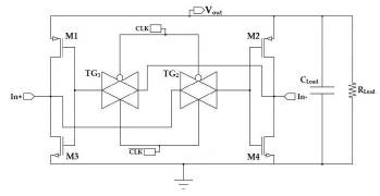
Figure 3
Architecture of the proposed rectifier with transmission gates.
Figure 4 shows a CMOS transmission gate that operates as an electronic switch controlled by a logic level, allowing to pass signals in both directions [17]. In the proposed topology, both transmission gates TG1 and TG2 can forward the current signal from the input to the output, i.e., there is a switching control from a closed to an open condition of the analog signal [18]. In the proposed rectifier circuit, TG1 and TG2 operate as short circuits when they have zero gate voltage, resulting in a negative voltage converter. Thus, the difference in the voltage of the piezoelectric transducer (connected to In+ and In-) allows conduction at M1 and M4 or M2 and M3, for variations of positive and negative voltage in the input signal, respectively [19]. This minimizes the voltage drop and leakage current of the CMOS cross-coupled rectifier.
![Transmission gate (TG) [17].](../2145-8456-uisi-21-01-103-gf4.jpg)
Figure 4
Transmission gate (TG) [17].
2.3. Layout of the CMOS rectifier
Figure 5 depicts the layout of the geometric pattern of the proposed rectifier based on 0.18Lim CMOS technology, considering a total silicon area of 54.765 μm x 86.355 μm.
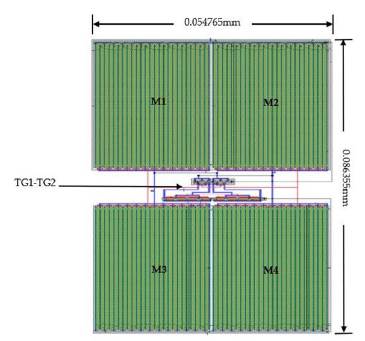
Figure 5
Layout of the proposed CMOS rectifier with transmission gates.
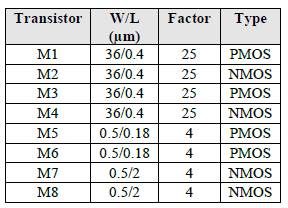
Table 1 indicates the aspect ratio of the transistors in our CMOS rectifier, which are determined using numerical simulations through T-Spice software.
2.4. Layout of the CMOS rectifier
To predict the VCE and PCE of the proposed CMOS rectifier, we used numerical simulations with T-Spice software. For this, a model of the piezoelectric transducer circuit of the energy harvester is required. This circuit supplies the electrical signal that is rectified [20], [21].
Figure 6 shows the equivalent electric circuit to a piezoelectric transductor, which consists of a capacitance (Cp) and parasitic resistance (Rp) in parallel with a source of sinusoidal current (ip(t) = IPs\n(2πfPt)). For this, IP varies with the mechanical excitation level of the piezoelectric transductor and fP represents its frequency [21].
![Electric circuit equivalent to a piezoelectric transductor [21].](../2145-8456-uisi-21-01-103-gf6.jpg)
Figure 6
Electric circuit equivalent to a piezoelectric transductor [21].
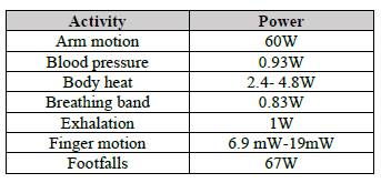
The human body can produce energy, which is generated by motion and body heat. Thus, possible to convert 1% of power from the human body can be enough to energy a wearable device [22]. Table 2 shows the sources of the human body.
For the simulation of the proposed rectifier with transmission gates, the following piezoelectric transductor parameters are used: IP= 125 μA, fP = 200 Hz, Cp = 25 nF, Rp = 1 MΩ. In addition, a TSMC 0.18μm CMOS technology model, obtained from MOSIS (Run: T18H), and a load resistance of 45 kΩ are used. This resistance represents the load of a wearable sensor [9].
Figure 7 depicts the waveforms ( ) of the control signals of the transmission gates. Also, it shows the waveforms of the input voltage given by the piezoelectric transductor (500 mV), along with the rectified voltage signal (Vout) and the output current signal of the rectifier (Iout). To study the performance of the CMOS rectifier with the transmission gates, we used different input signals with a voltage range from 0.5 V to 3.3V (maximum voltage supported by the CMOS technology). The rectified voltage (Vout) approaches the input voltage of the piezoelectric transductor (Fin), achieving an increase in the VCE and the PCE of the proposed rectifier.
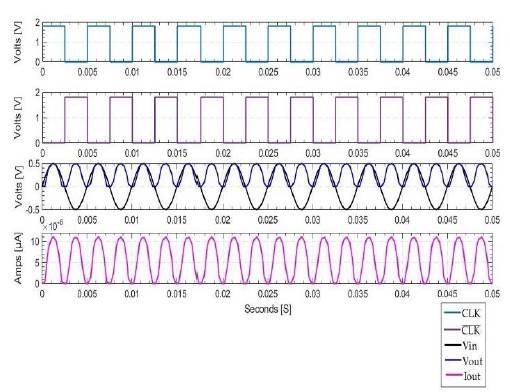
Figure 7
Simulation of the circuit of the proposed CMOS rectifier with transmission gate.
3. Results
The input and output signals, voltage and current, are used to determine the values of VCE and PCE of the CMOS rectifier, respectively. The VCE and PCE parameters are obtained with the following equations [13]:
Thus, input power is calculated with the RMS values of the input current and voltage during several period cycles. Output power is calculated by measuring the average output voltage of the rectified signal and dividing the square of this value by the charge resistance (Rload) [13].
Figure 8 shows a comparison of the relation between the input and output voltages of the proposed rectifier and a standard rectification circuit (D1N4148 diodes bridge). Both rectifiers are simulated using the same initial conditions of the piezoelectric transductor.
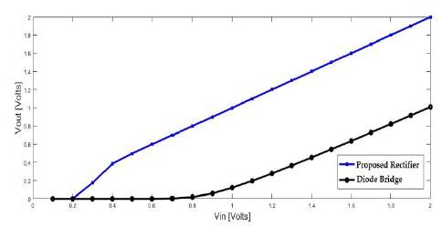
Figure 8
Results of the ratio of the input (VIN) and output (VOUT) voltages of the proposed CMOS rectifier and a D1N4148 diode bridge circuit.
We observed that a circuit with a diode bridge begins its rectification at 0.7 V. In our rectifier circuit, the rectification signal begins at 0.2 V. A significant response of VCE and PCE of the rectifier is obtained beginning at 0.5 V. However, the results indicate that at 0.3 V there is already an acceptable rectification. In addition, we compared the results of the VCE of our CMOS rectifier and the D1N4148 diodes bridge circuit, as shown in Figure 9. For this, we considered a Vin of 500mV and obtained a VCE of 99.4% for our rectifier. Thus, the VCE of the proposed rectifier is higher than that of the commercial diodes bridge circuit.
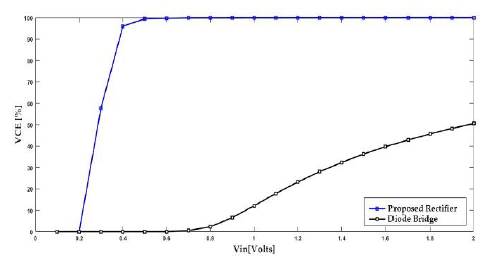
Figure 9
Results of the VCE of proposed CMOS rectifier and a D1N4148 diode bridge circuit. For both rectifier circuits, a frequency of 200Hz and a load resistance of 45 KΩ were considered.
Figure 10 depicts the results of the PCE of both the proposed CMOS rectifier and standard rectification circuit. The CMOS rectifier achieves a PCE up to 63.3% for an input signal of 500mV, resulting in a slight drop in power when a voltage higher than Vin is applied and maintaining an efficiency close to 58%. The PCE of the commercial diodes bridge circuit achieved a maximum value of about 25%, which is smaller than the values of the proposed CMOS rectifier.
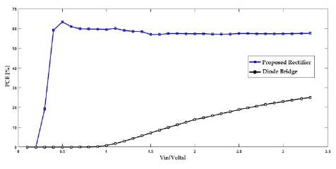
Figure 10
Results of the PCE of proposed CMOS rectifier and a D1N4148 diode bridge circuit. For both rectifier circuits, a frequency of 200Hz and a load resistance of 45 kΩ were considered.
Table 3 indicates the values for VCE and PCE of the proposed CMOS rectifier in comparison with other rectifiers reported in the technical literature [9], [21], [23]. These systems use active rectifiers. Based on the simulation results, the proposed rectifier has a higher VCE (99.4%) and lower size than those reported by [9], [23], [24].
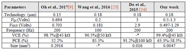
In addition, our rectifier achieves a PCE range from 58% to 63% for input voltage signals less than 1 V, which provides superior performance to commercial diode bridge rectifiers. Our CMOS rectifier has an acceptable performance to use in wearable piezoelectric energy harvesters.
Figure 11 shows a schematic view of a simple wearable piezoelectric energy harvester with the proposed CMOS rectifier. The cantilever beam may be a surface area of 1mm2 and is placed at the center of p-type substrate silicon. The beam will be including substrate silicon (50 x 14 x 12 μm), a zinc oxide (ZnO) layer (40 x 14 x 1 μn), an aluminum electrode (4 x 4 x 1 μm), and a seismic mass (5 x 14 x 20 μm).
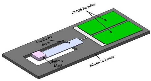
Figure 11
Schematic view of a simple wearable piezoelectric energy harvester with the proposed CMOS rectifier.
4. Conclusions
The design of a rectifier circuit based on 0.18μm CMOS TSMC technology with transmission gates is presented. This CMOS rectifier can be used for signal conditioning of piezoelectric energy harvesters of wearable devices. This rectifier was designed with a geometrical pattern of 54.765 μm x 86.355 μm, which included two transmission gates with four rectifiers transistors. The proposed signal conditioning circuit can rectifier input voltages up to 3.3 V. The VCE and PCE of the CMOS rectifier were increased to 99.4% and 63%, which represented better results than those of commercial diodes bridge circuit. The two transmission gates of the rectifier decrease its voltage drop using crossed coupling gates, registering an output power of 4.97μW with a load resistance of 45 kΩ. This rectifier can help to increase the charging efficiency of the harvested energy, decreasing the electrical energy losses. This could allow the increase in the energy supplied to wearable devices.
Acknowledgments
This work was supported by the Program of Doctorate in Applied Engineering of universidad Veracruzana and CONACYT through Grant 922430.
Reference
A. Goldberg, J. W. K. Ho, "Hactive: a smartphone application for heart rate profiling," Biophys. Rev., vol. 12, no. 4, pp. 777-779, 2020, doi: https://doi.org/10.1007/s12551-020-00731-3.
S. Ardalan, M. Hosseinifard, M. Vosough, H. Golmohammadi, "Towards smart personalized perspiration analysis: An IoT-integrated cellulose-based microfluidic wearable patch for smartphone fluorimetric multi-sensing of sweat biomarkers," Biosens. Bioelectron., vol. 168, pp. 112450, 2020, doi: https://doi.org/10.1016/j.bios.2020.112450.
S. B. Baker, W. Xiang, I. Atkinson, "Internet of Things for Smart Healthcare: Technologies, Challenges, and Opportunities," in IEEE Access, vol. 5. Institute of Electrical and Electronics Engineers Inc., 2017, pp. 26521-26544, doi: https://doi.org/10.1109/ACCESS.2017.2775180.
W. Tang, J. Ren, K. Deng, Y. Zhang, "Secure Data Aggregation of Lightweight E-Healthcare IoT Devices with Fair Incentives," IEEE Internet Things J., vol. 6, no. 5, pp. 8714-8726, 2019, doi: https://doi.org/10.1109/JIOT.2019.2923261.
A. M. Elmisery, S. Rho, M. Aborizka, "A new computing environment for collective privacy protection from constrained healthcare devices to IoT cloud services," Cluster Comput., vol. 22, no. 1, pp. 1611-1638, 2019, doi: https://doi.org/10.1007/s10586-017-1298-1.
A. S. Dahiya et al., "Energy autonomous wearable sensors for smart healthcare: A review," Journal of The Electrochemical Society, vol. 167, no. 3, pp. 037516, 2019, doi: https://doi.org/10.1149/2.0162003jes.
X. Li, E. S. Rogers, S. Nabavi, L. Zhang, "Effect of Varying Threshold Voltage on Efficiency of CMOS Rectifiers for Piezoelectric Energy Harvesting Applications," in Canadian Conference on Electrical and Computer Engineering , 2020, vol. 2020-August, doi: https://doi.org/10.1109/CCECE47787.2020.9255679.
W. L. Wu, C. Y. Yang, D. A. Wang, "A Flipping Active-Diode Rectifier for Piezoelectric-Vibration Energy-Harvesting," in 2020European Conference on Circuit Theory and Design (ECCTD), Sep. 2020, pp. 14, doi: https://doi.org/10.1109/ECCTD49232.2020.9218313.
T. Oh, S. K. Islam, G. To, M. Mahfouz, "Powering wearable sensors with a low-power CMOS piezoelectric energy harvesting circuit," in 2017IEEE International Symposium on Medical Measurements and Applications, MeMeA 2017 - Proceedings, Jul. 2017, pp. 308-313, doi: https://doi.org/10.1109/MeMeA.2017.7985894.
H. Lee, J. S. Roh, "Charging device for wearable electromagnetic energy-harvesting textiles," Fash. Text., vol. 8, no. 5, pp. 1-10, 2021, doi: https://doi.org/10.1186/s40691-020-00233-6.
A. Virattiya, B. Knobnob, M. Kumngern, "CMOS precision full-wave and half-wave rectifier," in Proceedings - 2011 IEEE International Conference on Computer Science and Automation Engineering, CSAE 2011, vol. 4, pp. 556-559, doi: https://doi.org/10.1109/CSAE.2011.5952911.
N. A. Wahab, M. K. M. Salleh, N. Othman, M. F. A. Khalid, N. M. Hidayat, "High efficiency CMOS rectifier for energy harvesting," in IEACon 2016 - 2016 IEEE Industrial Electronics and Applications Conference, 2017, pp. 123-127, doi: https://doi.org/10.1109/IEACON.2016.8067367.
H. K. Cha, W. T. Park, M. Je, "A CMOS rectifier with a cross-coupled latched comparator for wireless power transfer in biomedical applications," IEEE Trans. Circuits Syst. II Express Briefs, vol. 59, no. 7, pp. 409-413, 2012, doi: https://doi.org/10.1109/TCSII.2012.2198977.
S. Guo, H. Lee, "An efficiency-enhanced CMOS rectifier with unbalanced-biased comparators for transcutaneous-powered high-current implants," IEEE J. Solid-State Circuits, vol. 44, no. 6, pp. 1796-1804, 2009, doi: https://doi.org/10.1109/JSSC.2009.2020195.
X. D. Do, C. J. Jeong, H. H. Nguyen, S. K. Han, S. G. Lee, "A high efficiency piezoelectric energy harvesting system," in 2011International SoC Design Conference, ISOCC 2011, pp. 389-392, doi: https://doi.org/10.1109/isocc.2011.6138792.
G. D. Szarka, B. H. Stark, S. G. Burrow, "Review of power conditioning for kinetic energy harvesting systems," IEEE Transactions on Power Electronics, vol. 27, no. 2. pp. 803-815, 2012, doi: https://doi.org/10.1109/TPEL.2011.2161675.
M. M. Mano, M. D. Ciletti, Diseño Digital. 5th ed. Pearson Education: Ciudad de México, México, 2013.
R. J. Tocci, N. S. Widmer, G. L. Moss, Sistemas Digitales Principios y Aplicaciones. 8th ed. Pearson Education: Ciudad de México, México , 2017.
A. Costilla Reyes, A. Abuellil, J. J. Estrada-Lopez, S. Carreon-Bautista, E. Sanchez-Sinencio, "Reconfigurable system for electromagnetic energy harvesting with inherent activity sensing capabilities for wearable technology," IEEE Trans. Circuits Syst. II Express Briefs, vol. 66, no. 8, pp. 1302-1306, 2019, doi: https://doi.org/10.1109/TCSII.2018.2884613.
Y. Sun, I. Y. Lee, C. J. Jeong, S. K. Han, S. G. Lee, "An comparator based active rectifier for vibration energy harvesting systems," in 13aInternational Conference on Advanced Communication Technology, ICACT, 2011, pp. 1404-1408.
T. Oh, S. K. Islam, M. Mahfouz, G. To, "A Low-Power CMOS Piezoelectric Transducer Based Energy Harvesting Circuit for Wearable Sensors for Medical Applications," J. Low Power Electron. Appl., vol. 7, no. 4, pp. 33, 2017, doi: https://doi.org/10.3390/jlpea7040033.
L. Huang et al., "Fiber-Based Energy Conversion Devices for Human-Body Energy Harvesting," Adv. Mater., vol. 32, no. 5, pp. 1902034, 2020, doi: https://doi.org/10.1002/adma.201902034.
J. Wang, Z. Yang, Z. Zhu, Y. Yang, "An ultra-low-voltage rectifier for PE energy harvesting applications," J. Semicond., vol. 37, no. 2, pp. 025004, 2016, doi: https://doi.org/10.1088/1674-4926/37/2/025004.
X. D. Do , H. H. Nguyen, S. K. Han, D. S. Ha, S. G. Lee, "A self-powered high-efficiency rectifier with automatic resetting of transducer capacitance in piezoelectric energy harvesting systems," IEEE Trans. Very Large Scale Integr. Syst., vol. 23, no. 3, pp. 444-453, 2015. doi: https://doi.org/10.1109/TVLSI.2014.2312532.
Notes
Author notes
aEmails: rjuarez@uv.mxbrwoo@uv.mxcfrlopez@uv.mx. dprarlu@gmail.comeleherrera@uv.mx.