High-Performance 4 x 1 Multiplexer based on Single-Walled Carbon Nanotube Field Effect Transistor with CMOS-like Pass-Transistor Logic
Multiplexor 4 × 1 de alto rendimiento basado en un transistor de efecto de campo de nanotubos de carbono de pared simple con lógica de transistor de paso similar a CMOS
 Hamed Fooladvand h.fooladvand91@ms.tabrizu.ac.ir
Karim Abbasian k_abbasian@tabrizu.ac.ir
Hamed Baghban h-baghban@tabrizu.ac.ir
Hamed Fooladvand h.fooladvand91@ms.tabrizu.ac.ir
Karim Abbasian k_abbasian@tabrizu.ac.ir
Hamed Baghban h-baghban@tabrizu.ac.ir
High-Performance 4 x 1 Multiplexer based on Single-Walled Carbon Nanotube Field Effect Transistor with CMOS-like Pass-Transistor Logic
Revista INGENIERÍA UC, vol. 27, núm. 3, pp. 294-303, 2020
Universidad de Carabobo
Recepción: 26 Octubre 2020
Aprobación: 25 Noviembre 2020
Abstract: In the current research, the best property of Carbon Nanotube Field Effect Transistors (CNTFETs) exploited to propose a high performance 4-input 1-output (4 × 1) Multiplexer, using a CMOS-like Pass Transistor Logic (PTL) design style. To enhance a significant reduction in circuit complexity and a corresponding improvement in the performance envelope (power, area and speed) with respect to conventional CMOS equivalent circuit. The operating principles and experimental results for the PTL circuits using both p-FET and n-FET of CNTFETs presented. This property can be used in a multiplexer circuit, which transfers one of several input data to the output according to the control signal values. Results demonstrated that using of CNTFET can be achieved by constructing high performance carbon nanotube-based integrated circuits like logic Multiplexer based on a pass-transistor logic configuration. Further, this circuits can assembly with other circuits based on other Field effect transistors technology like GNR-FETs and improve ALU (Arithmetic Logic Unit) section of many processor ICs in high level of Nano-Scale VLSIs. The simulation results presented, and the power consumption compared with the conventional CMOS designs. The comparison of results approved that the CNTFET based design is capable of efficient power savings and high-speed performance.
Keywords: Carbon Nanotube Field Effect Transistor, Multiplexer, CMOS-like Pass Transistor Logic, Time Delay, PDP.
Resumen: En los últimos años, según muchos estudios, el transistor de efecto de campo de nanotubos de carbono (CNTFET) mostró un alto rendimiento en muchos circuitos lógicos debido a sus propiedades y en comparación con otros homólogos de silicio. Sin embargo, garantizar estos beneficios sigue siendo un desafío para la aplicación de circuitos integrados a nanoescala. Debido a sus excelentes características eléctricas y mecánicas, CNTFET es uno de los sustitutos más prometedores de la tecnología de transistores de efecto de campo semiconductores de óxido metálico (MOSFET). Aunque estas características son adecuadas para implementar en varios circuitos digitales prácticos, los circuitos basados en CNTFET resolverán enormes problemas de fabricación debido a su tamaño. En este artículo, mostramos que se podría obtener una simplificación importante mediante el diseño de circuitos integrados basados en CNTFET a través de una configuración lógica de transistor de paso tipo CMOS en el uso de transistores de efecto de campo, en lugar de la configuración tradicional de semiconductores de óxido de metal complementario (CMOS). La configuración PTL similar a CMOS crea una simplificación notable del diseño del circuito basado en CNTFET, una mayor velocidad del circuito y una gran reducción en el consumo de energía. Hay muchos problemas que se enfrentan al integrar un alto nivel de muchos transistores, como el efecto de canal corto, la disipación de potencia, el escalado de los transistores, etc. Para superar estos problemas, los Nanotubos de Carbono (CNT) tienen aplicaciones prometedoras en el campo de la electrónica. Los resultados de la simulación presentados y el consumo de energía en comparación con los diseños CMOS convencionales. La comparación de resultados probó que el diseño basado en CNTFET es capaz de ahorrar energía de manera eficiente y un rendimiento de alta velocidad.
Palabras clave: transistor de efecto de campo de nanotubos de carbono, multiplexor, lógica de transistor de paso tipo CMOS.
1. Introduction
In the past several years, according to many studies Carbon Nanotube Field Effect Transistor (CNTFET) shown high performance in many logic circuits due to their properties and compared with other silicon counterparts. However, ensuring these benefits still are as a challenge for nanoscale integrated circuits application. Because of its superb electrical and mechanical features, CNTFET is one of the most promising substitutes of metal–oxide–semiconductor field-effect transistor (MOSFET) technology. Although these features are suitable for implementing in various practical digital circuits, CNTFET-based circuits will solve enormous fabrication problems due to their size. Here, we show that a major simplification could be obtained by CNTFET based integrated circuits designing based on a CMOS-like pass-transistor logic configuration in the use of field effect transistors, instead of traditional Complementary Metal Oxide Semiconductor (CMOS) configuration. The CMOS-like pass transistor logic configuration creates a notable simplification of the CNTFET based circuit design, a higher circuit speed and great reduction in energy consumption. There are many issues facing while high level integrating many numbers of transistors such as short channel effect, power dissipation, scaling of the transistors and etc. To overcome these problems considering Carbon Nanotube (CNT) have promising application in the field of electronics. Carbon Nanotube (CNT) is a pioneer of new materials technologies for electronic design because of its unique mechanical and electrical properties [1], [2]. CNTFET is the most promising technology to extend or complement traditional silicon technology due to three reasons: first, the operation principle and the device structure are similar to CMOS devices and it is possible to reuse the established CMOS design infrastructure. Second, it is also possible to reuse CMOS fabrication process. And the most important reason is that the CNTFET has the best experimentally demonstrated device current carrying ability to date. Semiconducting carbon nanotubes are considered to be promising channel materials for the next generation of Nanoelectronic semiconductors, especially, for a high efficiency of Field Effect Transistors (FETs) [3], [4].
Also, Carbon Nanotubes (CNTs) and Graphene Nanoribbons have received significant attention from the academia as well the industry. Ideal electronic and structural properties of these materials make them suitable for electronic applications. These quests for knowledge are because of the fact that the improvement of the application and addition may lead to the improvement of other circuits parameters derived from them. Time Delay, power consumption and complexity are among instance of such parameters [5], [6]. Due to great extent of CNTFET in processors application, a Multiplexer based on SWCNT-FET is used in various applications wherein multiple data can be transmitted using a single line. In addition the Multiplexer could be vital of processors as evidenced by its wide use in Arithmetic Logic Unit (ALU) [7], [8].
2. Carbon Nanotube Field Effect Transistor (CNTFET) implementation plan
CNTFET model that developed by Stanford University used for many previous types of researches in this area. Stanford model implements a circuit-compatible model for Single Walled Carbon Nanotube Field Effect Transistor and is simulated in HSPICE [9], [10].
The p-FET and n-FET component used in this paper are shown in Figure 1. This model characterized in a process simulation framework by TCAD interactive tools and then by inspiration of Stanford CNTFET model with a little change, the circuit simulation of a 4 × 1 logic Multiplexer designed. Thus, this model implements a circuit-compatible model for SWCNT-FET due to real data for our simulations and is implemented in HSPICE.
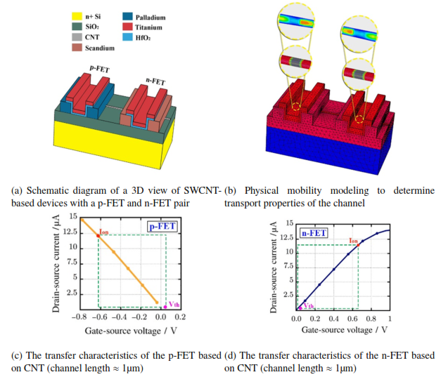
Figure 1
Structure and characteristics of n-type and p-type CNTFETs
Each CNTFET employs one SWCNT below its gate. The carbon nanotube under the both gates is identical. The part of the SWCNT directly under the gates is intrinsic, on the other hand, threshold voltage and output conductance exceedingly depend on the channel doping rate, thus for the doped source and drain parts of CNTFET, the doping level is taken as 0,85 % which is very higher than the first conduction band of the CNT. In this model, the screening effect of the charge in CNT under the gates can be ignored. Electron and hole mobility in CNT assumes equal. This design is simulated by 0,9 V operating voltage using HSPICE.
A schematic diagram showing a 3D view of SWCNT-based devices with a p-FET and n-FET pair is presented in Figure 1a. Physical mobility modeling with device simulation to determine transport properties of the channel shown in Figure 1b. The transfer characteristics of the p-FET and n-FET, based on the same CNT with a changeable diameter and a channel length of approximately 1 µm are shown in Figure 1c and Figure 1d. For the p-FET, the source is biased at 1,0 V and drain is at 0 V, whereas for the n-FET, the source is biased at 0 V and the drain is at 1,0 V.
The green box defines the gate voltage window used to obtain Ion, where Vth is determined using the standard peak trans-conductance method. The extracted Vth (pink point) and Ion (red point) are (Figure 1c) 0,05 V and 11,6 µA for the p-FET, and (Figure 1d) 0,03 V and 11,4 µA for the n-FET. The output characteristic of the p-type (orange line) and n-type (blue line) CNTFETs with |Vgs| varying from 0 to 1 V in steps of 0,2 V.
Figure 2 shows the operating principles for the Pass Transistor Logic (PTL) circuits using both p- and n-type of CNTFETs. As shown, when a low voltage (a logic 0, or 0 V) is applied to the gate for a p-FET pass transistor, Figure 2a, the resistance factor between the source (input) and drain (output) of the device, Rds, is on the order of 100 kΩ or less. Thus, the device is in its low-resistance or ON state, and may pass the input signal Vin from the source to the drain. When a high bias (a logic 1, which is 1,0 V) is applied to the gate Figure 2b, Rds is greater than 500 kΩ. The p-type device is thus in its high-resistance or OFF state and may not pass the input signal Vin to the output faithfully. The operation of an n-type pass transistor is similar to that of a p-type pass transistor, but in a complementary way. The n-type pass transistor can pass an input signal when a logic 1 is biased on the gate Figure 2c, and it is turned off when a logic 0 is biased on the gate Figure 2d. It should be noted that pass transistors are used here as switches to pass logic levels between the nodes of a circuit, rather than as switches connected directly to the power supply.
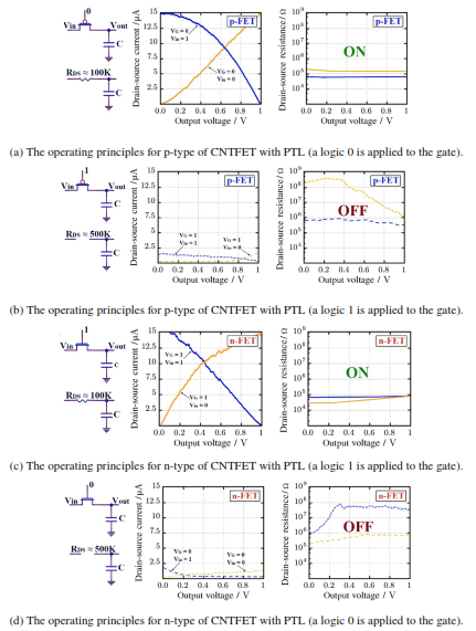
Figure 2
The operating principles of CNTFET-based PTL circuits
Pass transistor logic circuits based on CNTFET is a popular and widely used alternative to the conventional CMOS logic configuration, which can significantly reduce the number of transistors required to implement a logic circuit and has the additional advantage of lower capacitance [11], [12].
The main advantage of using PTL is that one Pass transistor (either a p-FET or an n-FET) is adequate to demonstrate a logical operation, which significantly reduces the number of transistors used than a circuit using a conventional CMOS configuration to achieve the same performance [13], [14]. One major drawback in the Silicon based PTL is that albeit an n-type pass transistor may produce a strong zero or ground, it produces only a weak logic one due to lowering the output below VDD–Vthn, where Vthn is the threshold voltage of the n-FET. On the other hand, a p-FET pass transistor produces a strong logic one, but a weak logic zero by raising the output above |Vthp| when the input is zero, where Vthp is the threshold voltage of the p-FET. This weak results from different threshold voltages for n-FET and p-FET, and the change in the output characteristics is usually known to as threshold voltage drop [15], [16]. One possible solution way to this deficiency is to regulate the threshold voltages of both the n-FET and p-FET, so that Vthn≈Vthp≈0 at the processing operation via doping. However, this is usually not acceptable in conventional silicon CMOS technology, but, the threshold voltage is readily adjustable in doping-free CNT CMOS-like technology [17]. Supplementary Figure 1 demonstrates that it is possible to change the threshold voltage of both n-FET and p- FET to the middle of them at approximately 0V by selecting a suitable gate metal, which greatly reduces the conventional threshold voltage in CNTFET-based PTL circuits. However, limited threshold voltage drops for both the n-type and p-type CNTFETs as pass transistors still prepared, as shown in Figure 2. For a p-FET Figure 2a, the output resistance for passing a logic 0 in its ON state (the solid orange line) is obviously larger than that for passing a logic 1 as the solid blue line. Thus, there still provides a small threshold voltage drop for the p-type CNTFET when a logic 0 is passed, and the voltage drop is significantly lower when passing a logic 1. In like manner, an n-type CNTFET passes a logic 0 well, while passing a logic 1 with a larger Rds, threshold drop at low bias Figure 2c.
However, advantaging from the small threshold voltage near zero, the threshold voltage drops for both n-type and p-type CNT pass transistors are much smaller than their conventional silicon counterparts, which show threshold voltages that are typically ten times larger [18], [19]. Fundamentally, these high- performance CNT pass transistors, many types of high-performance logic Integrated Circuits can be designed with a Pass Transistor Logic configuration [20], [21].
3. Multiplexer circuit implementation plan
Multiplexers are a common building block for data-paths and data-switching structures, and are used extensively in a number of applications including processors, processor buses, and network switches. The optimization of Multiplexer is at the heart of digital architecture performance tuning in terms of power, area and speed [22]. In the previous studies, various approaches have been proposed to reduce power consumption and the area in multiplexer section, the algorithm level and at the circuit level by defining the appropriate logic styles to match the application type. The use of CNTFET technology proved can be a promising alternative direction for this issue since such approaches have previously resulted in highly efficient solutions in term of power consumption, area and delay when used for standard or reconfigurable cells.
Here, we exploit the best property of CNTFETs to propose a high performance 4-input 1-output (4 × 1) Multiplexer, using a CMOS-like Pass Transistor Logic (PTL) design style, demonstrating a significant reduction in circuit complexity and a corresponding improvement in the performance envelope (power, area and speed) with respect to conventional CMOS equivalent circuit.
The operating principles and experimental results for the PTL circuits using both p-FET and n-FET of CNTFETs discussed in Figure 2, this property can be used in a Multiplexer circuit, which transfers one of several input data to the output according to the control signal values. This is shown in Figure 3 for an example Multiplexer with four data inputs A, B, C, D and two select inputs, S1 and S0, with the truth table.
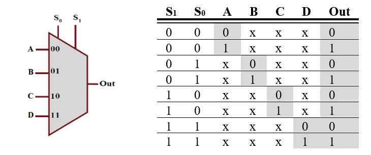
Figure 3
Truth table and graph for an ideal 4 × 1 Multiplexer
A sum of products implementation of the Multiplexer can be written like equation (1):
 (1)
(1)As shown in Figure 4, at a transistor level, this expression can be implemented with just six SWCNT- FET devices by CMOS-like pass transistor logic.
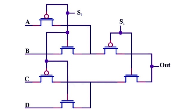
Figure 4
4 × 1 Multiplexer based on CNTFET with CMOSlike PTL
4. Performance evaluation
4.1. Simulation results
The input-output waveforms for proposed Multiplexer are shown in Figure 5. For example, when S1 and S0 have 1 and 0 logic value respectively, Multiplexer should show C logic value on output. This state can be investigated for other logic values due to Figure 5. Thus, our simulation results approved truth table near an ideal Multiplexer that shown in Figure 5. Meanwhile, Figure 6 shows a rising signal edge for output signal waveform of the multiplexer with more resolution in a very smaller time window that shows a high performance for CNTFET-based Multiplexer circuit design.
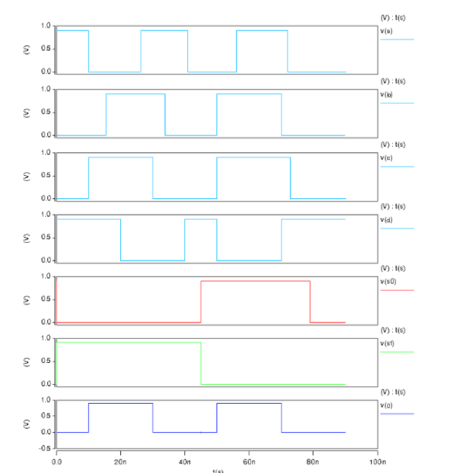
Figure 5
Input output signal waveforms for 4 × 1 Multiplexer
Generally, according Figure 5 graph V(a) is selected as V(o) when V(s1)=0 and V(s0)=0, whereas V(b) is selected when V(s1)=1 and V(s0)=0, V(c) is selected when V(s1)=0 and V(s0)=1, also V(d) is selected when V(s1)=1 and V(s0)=1.
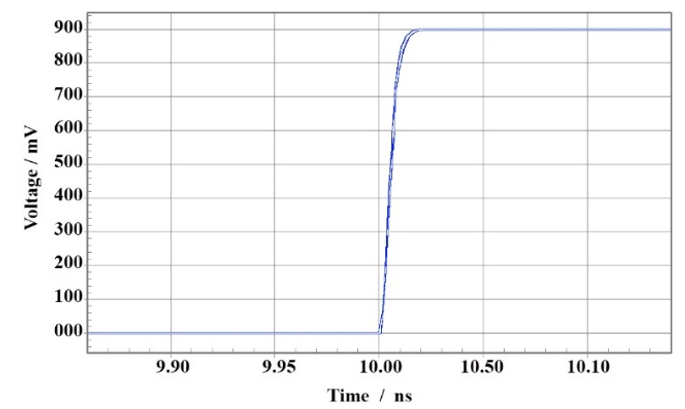
Figure 6
A rising signal edge of Multiplexer output waveform
4.2. Time Delay, Power consumption and PDP
Simulation results about time delay behavior of the CNTFET-based Multiplexer are shown in Table 1. The Power consumption of the CNTFETs with Power Delay Product (PDP) and PDP discrepancies values together are shown in Table 2.
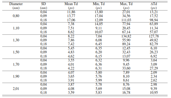
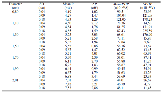
Where SD is standard deviation of CNT diameter, Td is time delay and ∆Td is propagation delay variation for presented circuit design.
Figure 7 shows simulation results of the Multiplexers according to diameter variation versus Time behavior. In this type of simulation, carbon nanotube diameter is swept from 0,60 nm to 2,20 nm and the various time delay criteria are estimated. Two important subjects can be obtained from Figure 8. The first subject is that dispersion in time delay, rise time and fall time all increase aggressively as CNT diameter is decreased to lower than 0,80 nm. Furthermore, when CNT diameter increases more than 0,80 nm point, the time delay is permanently decreased.

Figure 7
Multiplexer Timing Behavior according to CNT Diameter change
This means when carbon nanotube diameter increases, energy band gap is decreased as a result authorizing more charge carriers to participate in current transferring and increasing conduction, increasing the current through the CNT means that delay is permanently reduced till entering the balanced state at diameters larger than 1,5 nm while supply voltage fixed on 0,90 V. The second subject is about fall time and rise time that they are very similar and this issue approve that due the equal mobility of electrons and holes in CNT, utilizing structure with CNTFETs for a Multiplexer with Pass Transistor Logic would yield to similar rise time and fall time and uniform waveform.
Where SD is Standard Deviation of CNT diameter, Mean P is Mean Power consumption, ∆P is propagation Power consumption differences, PDP is Power Delay Product and ∆PDP is PDP discrepancies for presented circuit.
The quantitative simulation results of 4 × 1 Multiplexers shown in Figure 8. CNT diameter is swept from a minimum value to a maximum value (0,60 nm to 2,00 nm). As shown where carbon nanotube diameter increases, power consumption is increased, that is because of the energy band gap decreasing in CNT. When CNT diameter increases, its band gap is reduced, thus charge carriers need lower energy to flow and producing a greater current. This operation increased current successively and causes power consumption to increase. The graph shows a snap rise for power consumption where CNT diameter is increased above 1,5 nm.
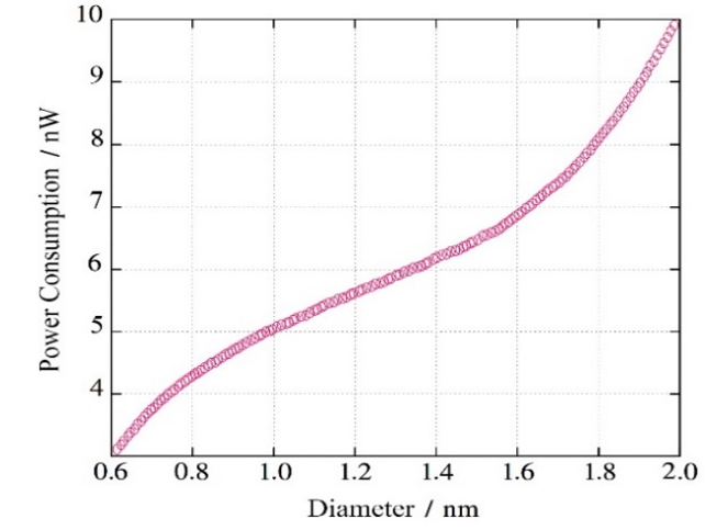
Figure 8
Power Consumption versus various diameter for 4 × 1 Multiplexer
Monte Carlo simulation results of 9500 Multiplexers shown in Figure 9. It illustrates the Multiplexers uncertain cases of Time delay propagation, it is drawn up according to differences in maximum and minimum rise time and fall time, carbon nanotube average diameter and standard deviation. The instability in delay for Multiplexer is critical when the small mean CNT diameter is blended with larger SDs of CNT diameter.

Figure 9
Multiplexer Delay time according to CNT diameter & SD variation
5. Discussion
It is well known that a good circuit configuration at the architectural level should take full advantage of the component device properties at the physical level. Here, we summarized the advantages of a 4 × 1 Multiplexer based on Single Wall Carbon Nanotube Field Effect Transistor with Pass Transistor Logic. Our design compared with other methods that presented in [23], [24] first, the number of transistors can be significantly reduced if a circuit with an optimal function is designed with a Pass Transistor Logic configuration when compared with that using the usual CMOS or other configurations as shown in Figure 10. Reducing the number of transistors in an IC not only leads to higher efficiency per transistor, but also to higher speed and lower static power dissipation overall. Second, the major drawback of conventional circuit threshold voltage drop is largely avoided in CNTFET-PTL circuit, because of the readily adjustable threshold voltage of the CNTFET.
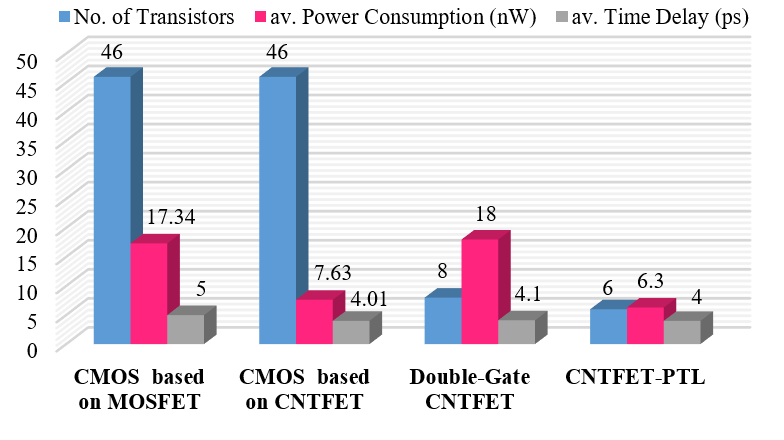
Figure 10
Comparison of average performance metrics for various 4 × 1 MUX
6. Conclusion
Using CNTFET can be achieved by constructing high-performance carbon nanotube-based integrated circuits like logic Multiplexer based on a pass-transistor logic configuration, which this circuits can assembly with other circuits based on other Field effect transistors technology like GNR-FETs and improve ALU (Arithmetic Logic Unit) section of many processor ICs in high level of Nano-Scale VLSIs.
The comparison of results indicated that the CNTFET based design is capable of efficient power savings. The 4 × 1 Multiplexer is designed using CNTFET with the different CNT diameters and the performance of the proposed designs are evaluated in various simulation conditions.
7. References
[1] K. Young Bok, K. Yong-Bin, and K. Lombardi, “A novel design methodology to optimize the speed and power of the CNTFET circuits,” in 2009 52nd IEEE International Midwest Symposium on Circuits and Systems, 2009, pp. 1130–1133.
[2] K. Yong-Bin, “Integrated circuit design using carbon nanotube field effect transistor,” Transactions on Electrical and Electronic Materials, vol. 12, no. 5, pp. 175–188, 2011.
[3] L. Sheng, K. Yong-Bin, and F. Lombardi, “A novel CNTFET-based ternary logic gate design.” in 2009 52nd IEEE International Midwest Symposium on Circuits and Systems, 2009, pp. 435–438.
[4] C. Geunho, K. Yong-Bin, F. Lombardi, and M. Choi, “Performance evaluation of CNFET-based logic gates,” in 2009 IEEE Instrumentation and Measurement Technology Conference, 2009, pp. 909–912.
[5] B. Jingwei and Y. Huang, “Fabrication and electrical properties of graphene nanoribbons,” Materials Science and Engineering: R: Reports, vol. 70, no. 3–6, pp. 341–353, 2010.
[6] M. Montazeri-Gh and M. Mahmoodi-K, “Optimized predictive energy management of plug-in hybrid electric vehicle based on traffic condition.” Journal of cleaner production, vol. 139, pp. 935–948, 2016.
[7] S. L. Murotiya and A. Gupta, “Design of CNTFET-based 2-bit ternary ALU for nanoelectronics,” International Journal of Electronics, vol. 101, no. 9, pp. 1244–1257, 2014.
[8] A. Sharma and T. Ravi, “Low power 8-bit ALU design using full adder and multiplexer,” in 2016 International Conference on Wireless Communications, Signal Processing and Networking (WiSPNET), 2016, pp. 2160–2164.
[9] J. Deng and H. S. P. Wong, “A compact SPICE model for carbon-nanotube field-effect transistors including nonidealities and its application—Part I: Model of the intrinsic channel region,” IEEE Transactions on Electron Devices, vol. 54, no. 12, pp. 3186–3194, 2007.
[10] L. Ding, Z. Zhiyong, P. Tian, L. Shibo, W. Sheng, Z. Weiwei, L. Jie, and P. Lian-Mao, “Carbon nanotube field-effect transistors for use as pass transistors in integrated logic gates and full subtractor circuits,” ACS Nano, vol. 6, no. 5, pp. 4013–4019, 2012.
[11] L. Ding, Z. Zhiyong, L. Shibo, P. Tian, W. Sheng, L. Yan, Z. Weiwei, L. Jie, and P. Lian-Mao, “CMOS-based carbon nanotube pass-transistor logic integrated circuits,” Nature Communications, vol. 3, p. 677, 2012.
[12] T. Pei, P. Zhang, Z. Zhang, C. Qiu, S. Liang, Y. Yang, S. Wang, and L. M. Peng, “Modularized construction of general integrated circuits on individual carbon nanotubes,” Nano Letters, vol. 14, no. 6, pp. 3102–3109, 2014.
[13] R. Zimmermann and W. Fichtner, “Low-power logic styles: CMOS versus pass-transistor logic,” IEEE Journal of Solid-State Circuits, vol. 32, no. 7, pp. 1079–1090, 1997.
[14] J. M. Rabaey, A. P. Chandrakasan, and B. Nikolić, Digital integrated circuits: a design perspective. Pearson Education, 2003, vol. 7.
[15] N. H. E. Weste and D. M. Harris, CMOS VLSI Design: A Circuits and System Perspective, 4th ed., M. Hirsch, Ed. Addyson-Wesley, 2005.
[16] Z. Zhang, S. Wang, L. Ding, X. Liang, T. Pei, J. Shen, H. Xu, Q. Chen, R. Cui, Y. Li, and L. M. Peng, “Self-aligned ballistic n-type single-walled carbon nanotube field-effect transistors with adjustable threshold voltage.” Nano Letters, vol. 8, no. 11, pp. 3696–3701, 2008.
[17] S. M. Sze and K. K. Ng, Physics of semiconductor devices, 3rd ed. John Wiley & sons, 2006.
[18] A. Chen, J. Hutchby, V. Zhirnov, and G. Bourianoff, Emerging nanoelectronic devices. John Wiley & Sons, 2014.
[19] Y. S. Mehrabani, F. M. Reza, and E. Mohammad, “A novel low-energy CNFET-based full adder cell using pass-transistor logic,” International Journal of High Performance Systems Architecture, vol. 5, no. 4, pp. 193–201, 2015.
[20] M. Grailoo, M. Hashemi, K. Haghshenas, S. Rezaee, S. Rapolu, and T. Nikoubin, “CNTFET full-adders for energy- efficient arithmetic applications,” in 2015 6th International Conference on Computing, Communication and Networking Technologies (ICCCNT), 2015, pp. 1–6.
[21] P. Metzgen, “A high performance 32-bit ALU for programmable logic,” in FPGA ’04: Proceedings of the 2004 ACM/SIGDA 12th international symposium on Field programmable gate arrays, 2004, pp. 61–70.
[22] K. Jabeur, I. O’Connor, N. Yakymets, and S. Le Beux, “High performance 4:1 multiplexer with ambipolar double-gate FETs,” in 2011 18th IEEE International Conference on Electronics, Circuits, and Systems, 2011, pp. 677–680.
[23] P. Sadeghpour and H. Mirzaei, “A 180 nm CMOS Low Noise Amplifier with Increased linearity using Current-Reuse Technique for Broadband Applications,” Journal of Research in Science, Engineering and Technology, vol. 7, no. 1, pp. 21–27, 2019.
[24] G. L. Madhumati, M. Madhavilatha, and K. Ramakoteswara Rao, “Power and delay analysis of a 2-to-1 multiplexer implemented in multiple logic styles for multiplexer-based decoder in Flash ADC,” International Journal of Recent Trends in Engineering, vol. 1, no. 4, pp. 29–31, 2009.
Enlace alternativo
http://servicio.bc.uc.edu.ve/ingenieria/revista/v27n3/art04.pdf (pdf)
https://www.revistas.uc.edu.ve/index.php/revinguc/article/view/149 (html)